Clock sources and methods with reduced clock jitter
a clock source and clock jitter technology, applied in the direction of generating/distributing signals, pulse techniques, instruments, etc., can solve the problems of excessive jitter of the clock signal about the intended temporal position, degrade the performance (e.g., signal-to-noise ratio) of the system that processes the samples, etc., to achieve the effect of reducing clock jitter
- Summary
- Abstract
- Description
- Claims
- Application Information
AI Technical Summary
Benefits of technology
Problems solved by technology
Method used
Image
Examples
embodiment 20
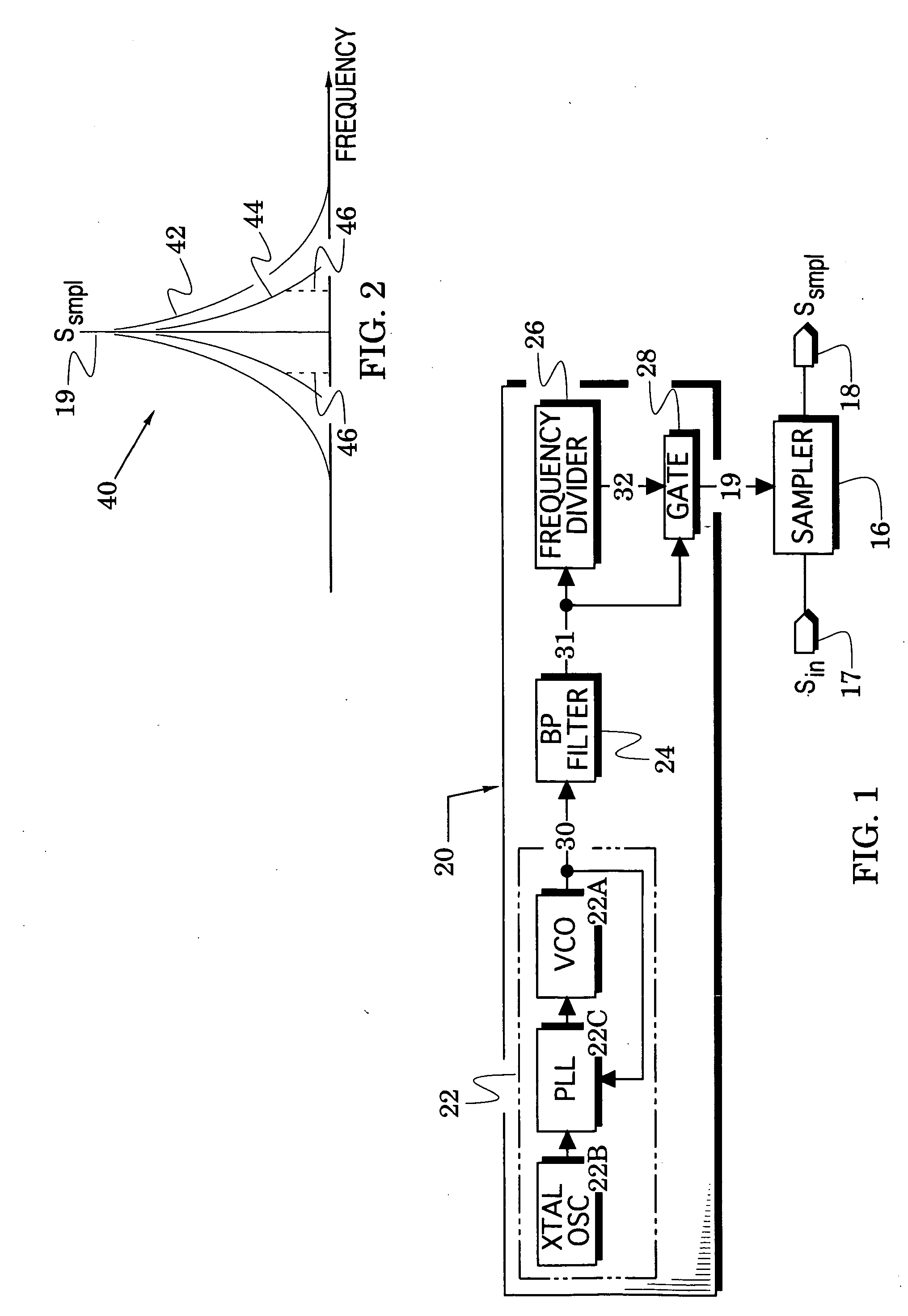
[0014] In particular, FIG. 1 illustrates a sampler 16 that receives an input analog signal Sin from an input port 17 and provides a sample Ssmpl of the analog signal to an output port 18 in response to each pulse of a clock signal 19 that is received from a clock source embodiment 20. The clock source 20 includes a signal generator 22 and a converter that comprises a bandpass filter 24, a frequency divider 26 and a gate 28.
[0015] In operation of the clock source 20, the signal generator generates a first signal 30 whose frequency is significantly elevated above the intended frequency of the clock signal 19 to thereby significantly increase its slew rate. FIG. 1 illustrates a signal generator 22 in which a voltage-controlled oscillator (VCO) 22A is phase locked to a crystal oscillator (XTAL OSC) 22B through a phase-locked loop (PLL) 22C. It is noted, however, that other clock source embodiments 20 may be realized with different embodiments of the signal generator 22.
[0016] The first...
embodiment 60
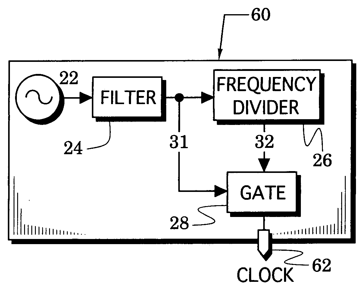
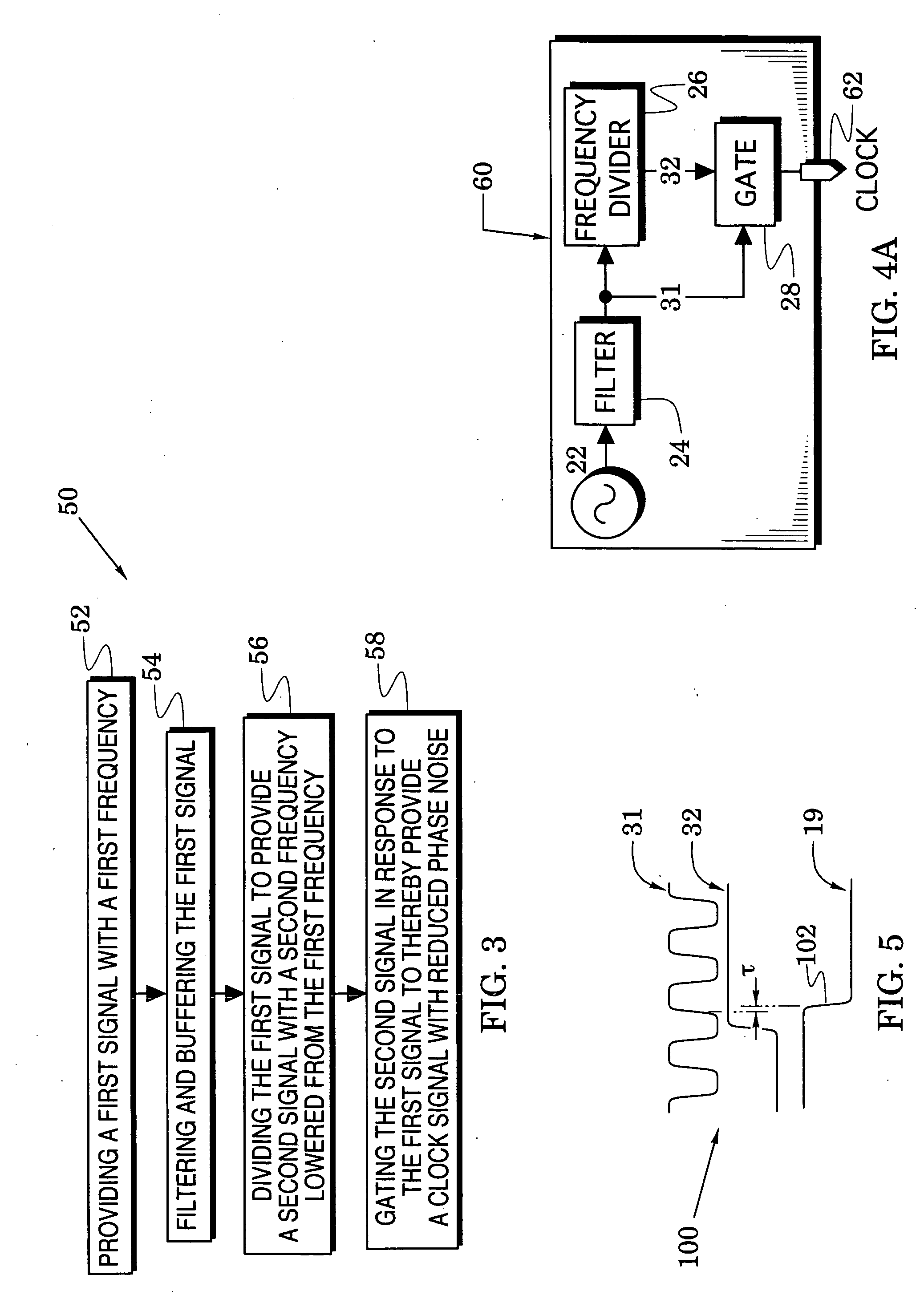
[0022]FIG. 4A illustrates a clock source embodiment 60 which uses some of the reference numbers of the clock source 20 of FIG. 1. As shown, the filter 24 filters a first signal that is provided by a signal source 22 to thereby provide a filtered first signal 31. Although the filter maintains the high slew rate of the first signal, it attenuates wide band noise. A frequency divider 26 divides the first signal with its first frequency to a second signal 32 with a lowered second frequency. The second signal is then gated to an output port 62 when the gate 28 responds to altered states of the first signal 31.
[0023] In more detail, FIG. 4B illustrates a clock source embodiment 60 which uses some of the reference numbers of the clock source 20 of FIG. 1. In particular, the clock source 60 includes a signal generator 22 that generates a first signal 30, a filter network 24 that converts the first signal 30 to a filtered first signal 31, and a frequency divider 26 that divides the first sig...
PUM
 Abstract
Description
Claims
Application Information


