Clock auto-phasing for reduced jitter

a clock and jitter technology, applied in the field of power supply noise reduction, can solve problems such as device malfunction, device supply voltage fluctuations, and device performance degradation, and achieve the effect of reducing clock jitter

Active Publication Date: 2012-09-04
XILINX INC
View PDF3 Cites 7 Cited by
  • Summary
  • Abstract
  • Description
  • Claims
  • Application Information

AI Technical Summary

Benefits of technology

[0011]By dynamically phase-shifting the triggering of switching events in the first circuit block in response to fluctuations in the device's supply voltage, embodiments of the present invention may more effectively reduce clock jitter resulting from power supply fluctuations than prior techniques that employ a static delay element. Embodiments of the present invention are particularly applicable to user-configurable devices such as PLDs for which the temporal relationship between switching events in the device's various circuit blocks are unknown when the device is fabricated and / or when the device is delivered to a customer. Further, because of the control circuit's dynamic nature, embodiments of the present invention may compensate for process variations inherent in the fabrication of semiconductor devices and / or for variations in operating temperature.

Problems solved by technology

As known in the art, undesirable fluctuations in the device's power supply (e.g., caused by switching noise, ground bounce, and the like) may create clock jitter in one or more of the device's circuit blocks, which in turn may not only degrade device performance but may also result in device malfunction.
For example, switching events such as logic state transitions of signals in CMOS circuits typically generate transient currents that may cause undesirable fluctuations in the device's supply voltage.
These undesirable supply voltage fluctuations may alter the timing characteristics of switching events in one or more of the device's circuit blocks, which in turn may result in timing errors.
For many IC devices, a significant portion of the supply voltage noise may be caused by switching events in a relatively small number of the device's circuit blocks.
Thus, if a number of first circuit blocks generate relatively small transient currents during switching events and a number of second circuit blocks generate relatively large transient currents during switching events, switching events in the second circuit blocks may cause supply voltage fluctuations that result in clock jitter in the first circuit blocks.
Unfortunately, the static delay element is unable to compensate for process variations inherent in the fabrication of semiconductor devices and / or for unpredictable variations in operating conditions such as, for example, operating temperature variations.
Further, the static nature of prior techniques is relatively ineffective for minimizing clock jitter in user-configurable IC devices such as programmable logic devices (PLDs).
For example, because a PLD is usually configured by a user to implement a specific circuit design, the PLD manufacturer is typically unaware of the temporal relationship between switching events in the various PLD resources that will be utilized to implement the user's design.
As a result, employing a static delay element in a user-configurable device such as a PLD to minimize clock jitter typically produces unpredictable results.

Method used


Image

  • Clock auto-phasing for reduced jitter
  • Clock auto-phasing for reduced jitter
  • Clock auto-phasing for reduced jitter

Examples


Embodiment Construction

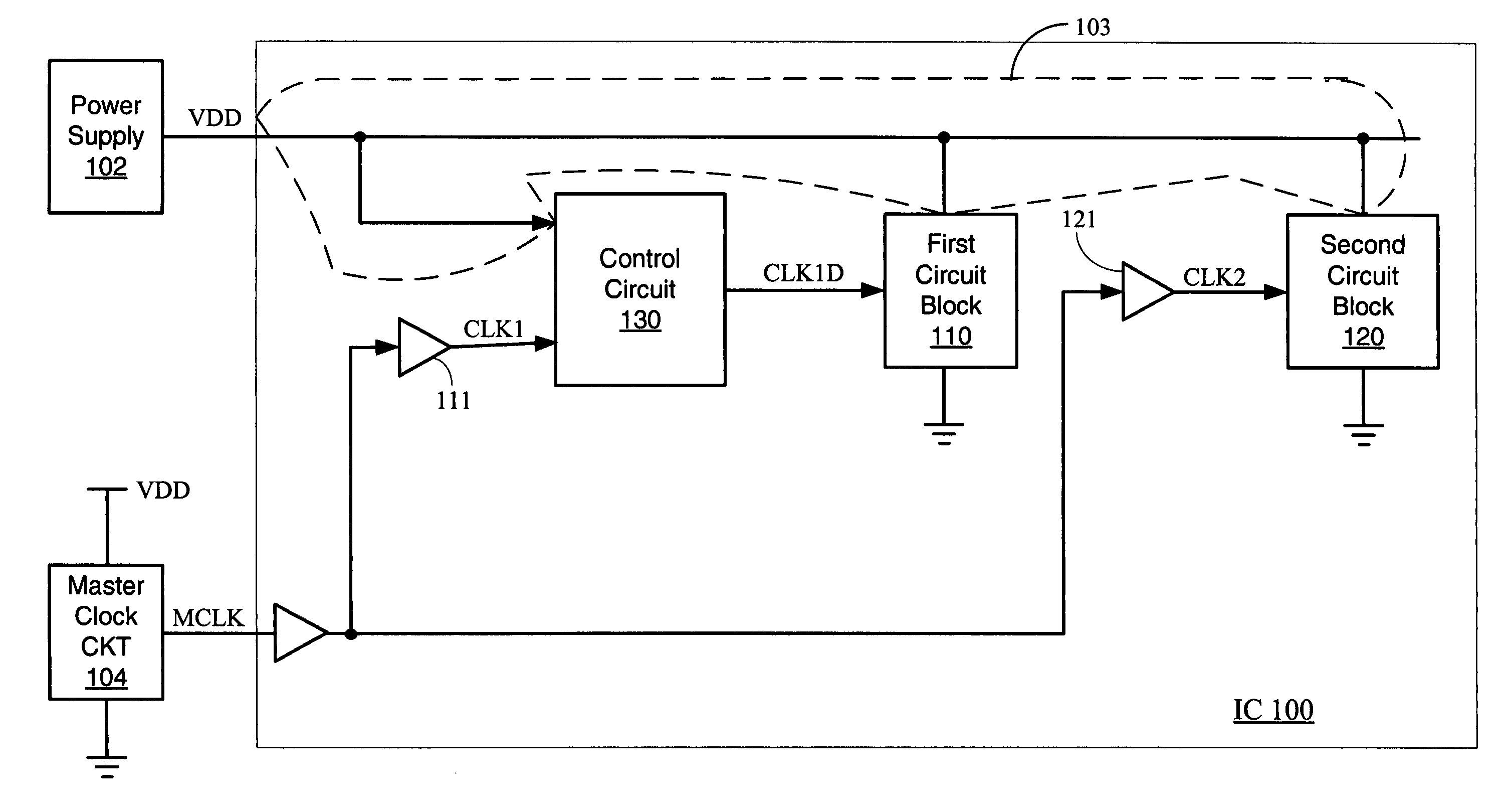
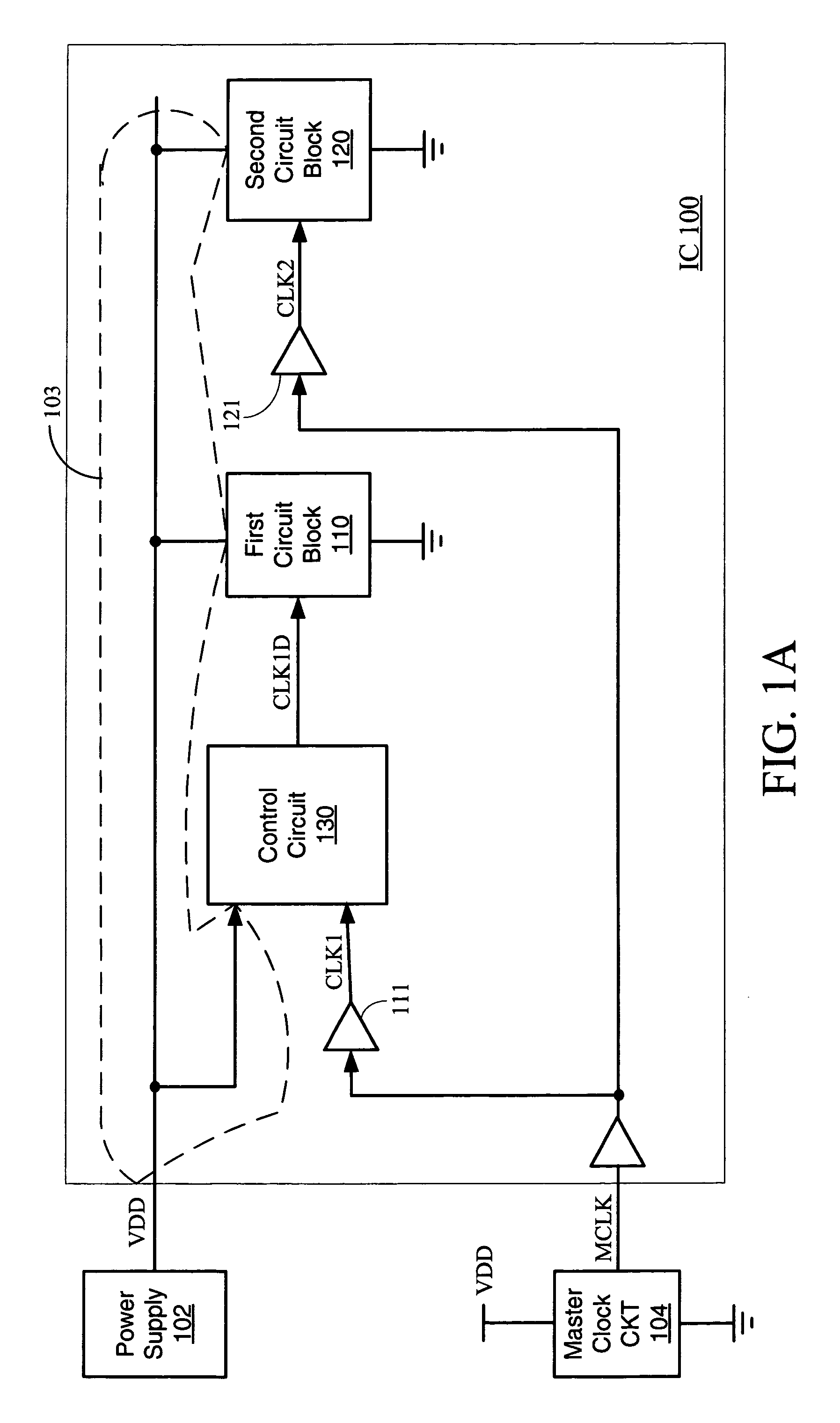
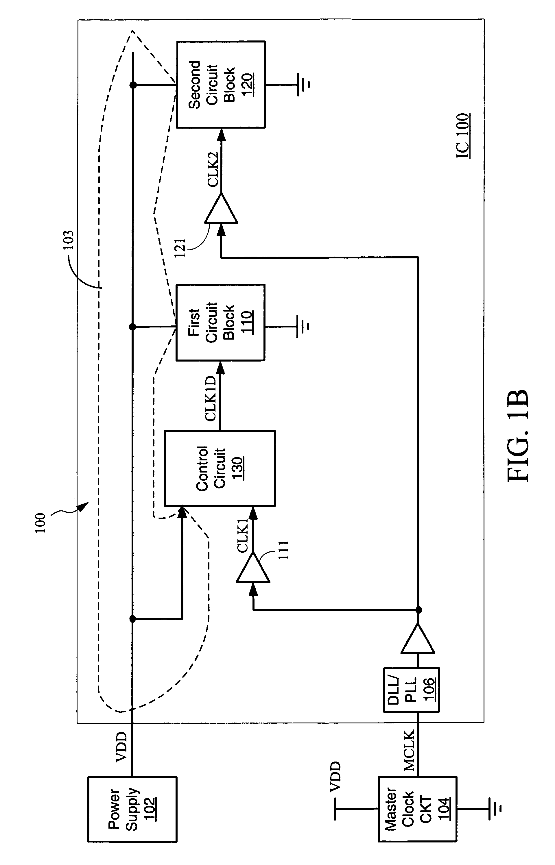
[0025]Embodiments of the present invention are described below in the context of an exemplary IC device 100 for simplicity only. It is to be understood that present embodiments are equally applicable to other IC devices including, for example, programmable logic devices (PLDs) such as Field Programmable Gate Arrays (FPGAs) and / or complex PLDs, application-specific integrated circuit (ASIC) devices, microprocessors, and other suitable semiconductor devices. In the following description, for purposes of explanation, specific nomenclature is set forth to provide a thorough understanding of the present invention. In other instances, well-known circuits and devices are shown in block diagram form to avoid obscuring the present invention unnecessarily. Further, although present embodiments are described below as being responsive to the rising edges of various clock signals, other embodiments may be responsive to either the falling edges or to both the rising and falling edges of the vario...


PUM


Abstract

The relative timing of triggering switching events in a circuit block of an IC device is dynamically adjusted in response to fluctuations in device's supply voltage to minimize clock jitter caused by supply voltage noise. A control circuit monitors supply voltage fluctuations, and in response thereto dynamically phase-shifts a clock signal that triggers the switching events so that the switching events occur during relatively quiet time intervals in which fluctuations in the supply voltage are minimal.

Description

FIELD OF INVENTION[0001]This invention relates generally to power supply noise in integrated circuit (IC) devices, and in particular to reducing clock jitter resulting from power supply noise.DESCRIPTION OF RELATED ART[0002]Digital IC devices typically employ a global or system clock signal to synchronize various synchronous circuit elements with each other. The system clock signal is typically distributed across an IC device via one or more global clock lines, and is often used to generate a number of local clock signals for clocking synchronous circuit elements in corresponding circuit blocks formed within the device. As known in the art, undesirable fluctuations in the device's power supply (e.g., caused by switching noise, ground bounce, and the like) may create clock jitter in one or more of the device's circuit blocks, which in turn may not only degrade device performance but may also result in device malfunction.[0003]For example, switching events such as logic state transiti...

Claims


Application Information

Patent Timeline
Patent Type & Authority Patents(United States)
IPC IPC(8): H03K3/00
CPCG06F1/10G06F1/28
Inventor ALEXANDER, MARK A.KOONTZ, SEAN A.
Owner XILINX INC
Why Eureka
Try Eureka