
Semiconductor device

Active Publication Date: 2015-10-01
RENESAS ELECTRONICS CORP
View PDF3 Cites 5 Cited by
  • Summary
  • Abstract
  • Description
  • Claims
  • Application Information

AI Technical Summary

Benefits of technology

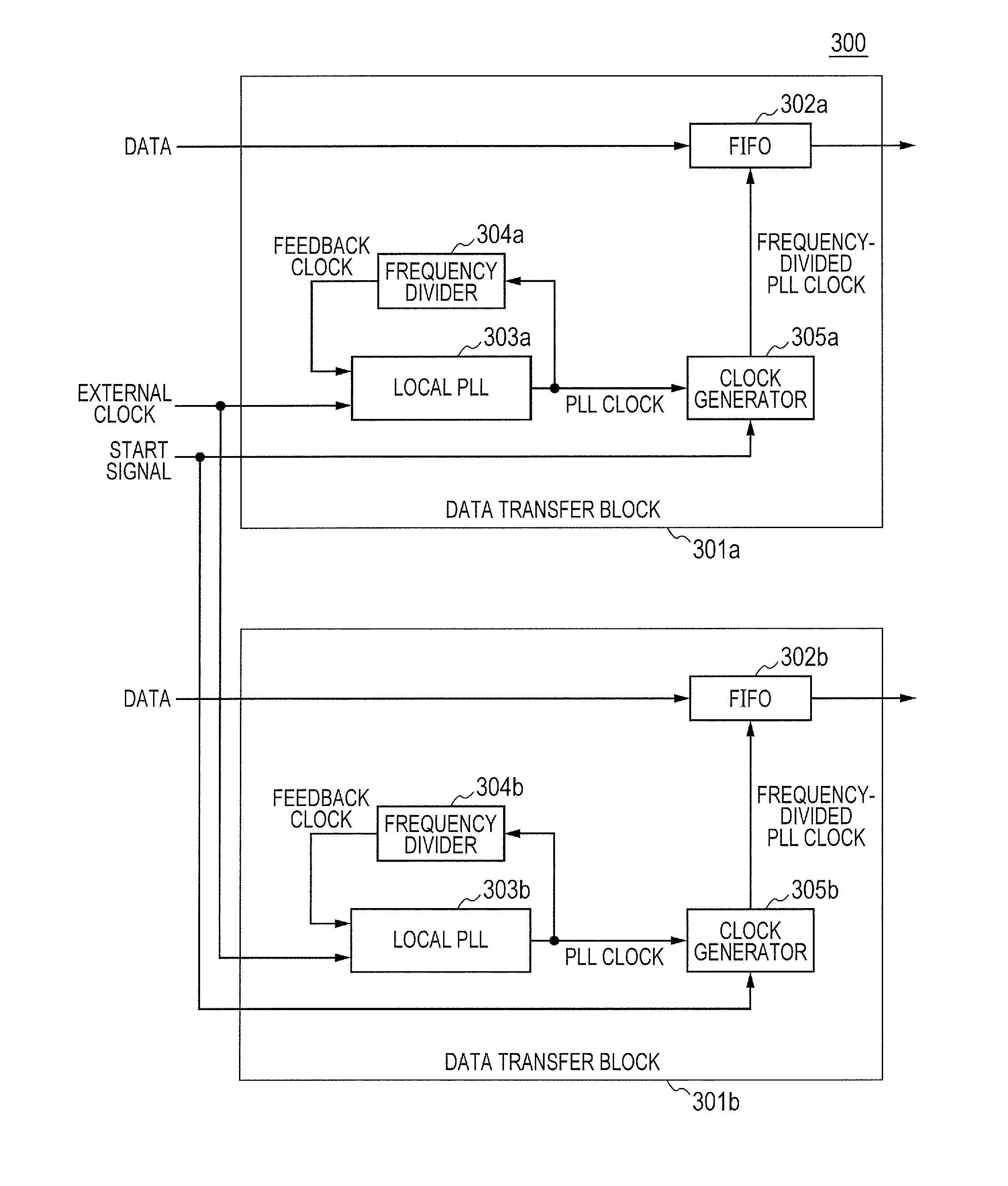
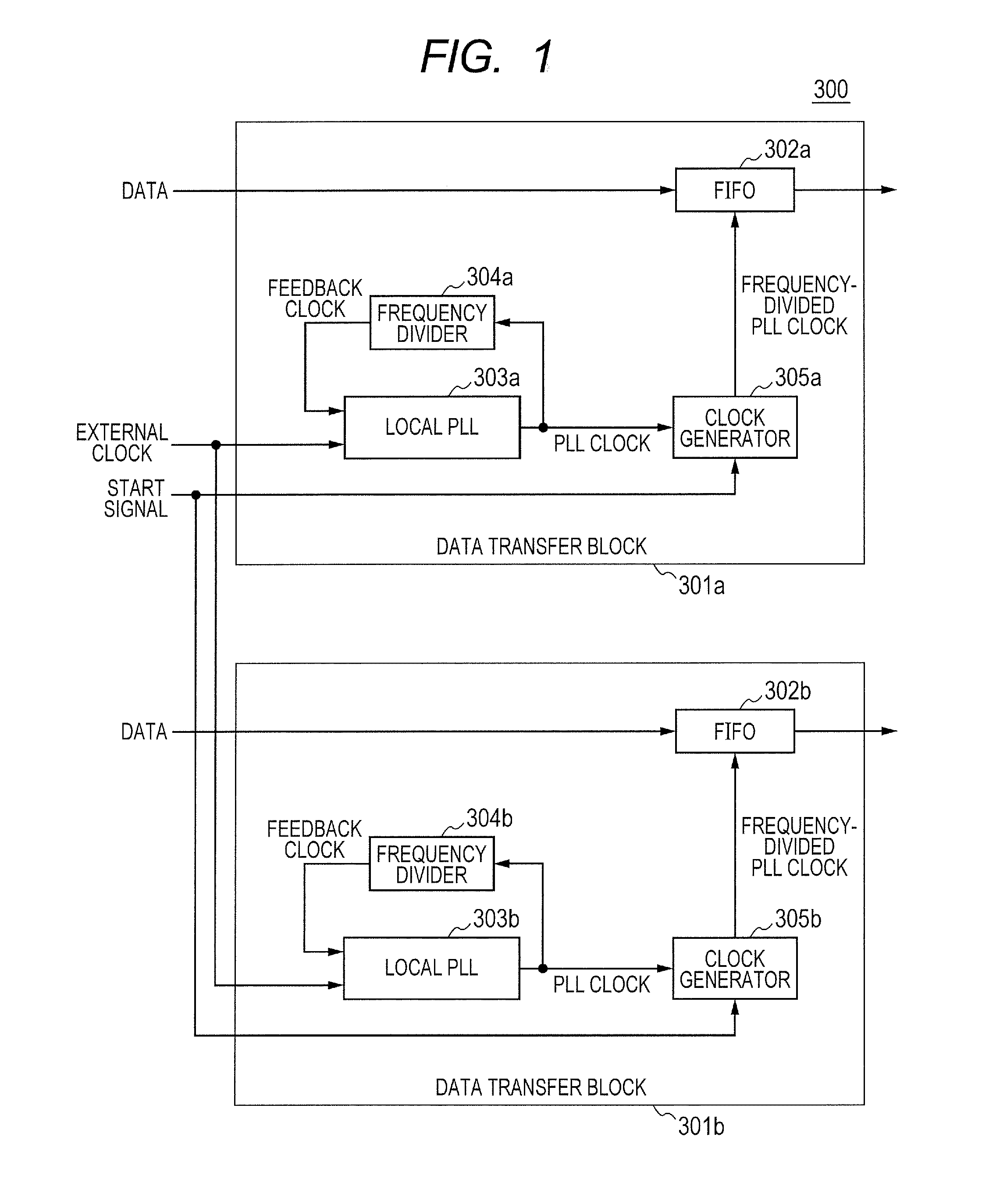
The present invention solves the problem of clock jitter by providing a plurality of data transfer blocks with local PLL circuits and controlling the phases of frequency-divided PLL clocks using a common start signal. This results in the same phases of clocks in each data transfer block. This improves the reliability and efficiency of advanced semiconductor devices such as servers and high-speed switches.

Problems solved by technology

Such a case has a problem that, when the distance between the data transfer blocks increases, the tree length of a clock supplied to each of the data transfer blocks becomes longer and a clock jitter becomes larger.
There is, however, a problem that the phases of clocks obtained by frequency-dividing PLL clocks output from the local PLL circuits cannot be made the same in the plurality of data transfer blocks.

Method used


Image

  • Semiconductor device
  • Semiconductor device
  • Semiconductor device

Examples


first embodiment

[0028]FIG. 1 is a diagram expressing the configuration of a semiconductor device according to a first embodiment of the present invention.

[0029]A semiconductor device 300 is obtained by forming integrated circuits on a single semiconductor chip.

[0030]The semiconductor device 300 has a plurality of data transfer blocks 301a and 301b. The two data transfer blocks 301a and 301b are disposed so as to be dispersed. For example, the data transfer block 301a is adjacently disposed along one of four sides of a semiconductor chip having a rectangular shape in plan view, and the data transfer block 301b is adjacently disposed along any of the other three sides including the opposed side in the semiconductor chip.

[0031]To the data transfer blocks 301a and 301b, a common external clock and a common start signal (also called a hint signal) are supplied.

[0032]The data transfer block 301a has a local PLL (Phase Locked Loop) circuit 303a, a frequency divider 304a, a clock generator 305a, and an FIF...

second embodiment

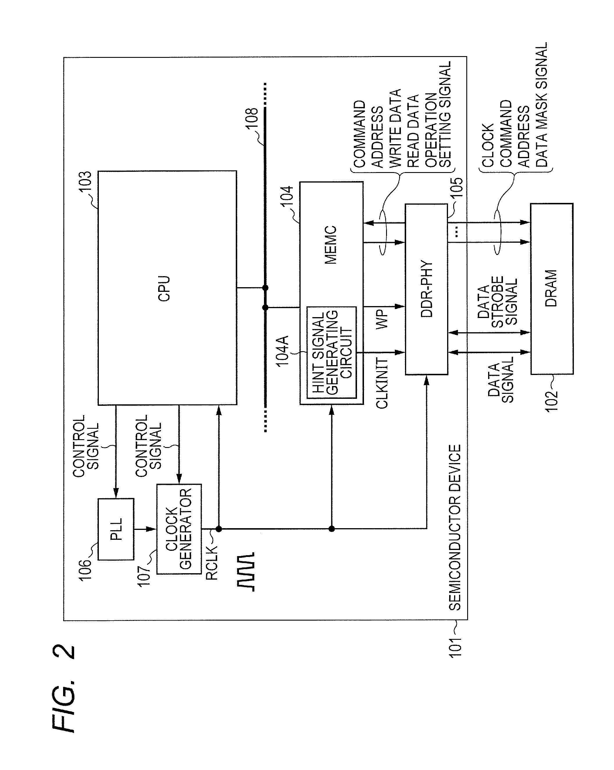
[0039]FIG. 2 is a diagram expressing the configuration of a semiconductor device according to a second embodiment of the present invention.

[0040]A semiconductor device 101 is obtained by forming integrated circuits on a single semiconductor chip. A DRAM (Dynamic Random Access Memory) 102 illustrated in FIG. 2 is configured by a semiconductor chip different from that of the semiconductor device 101.

[0041]The semiconductor device 101 is, for example, an SoC (System on Chip) as a component of a microcomputer, a baseband IC provided in a portable device, or an application processor.

[0042]As illustrated in FIG. 2, the semiconductor device 101 has a CPU (Central Processing Unit) 103, a PLL circuit 106, a clock generator 107, an MEMC (Memory Controller) 104, and a DDR-PHY 105.

[0043]The DDR-PHY 105 is coupled to the DRAM 102 on the outside. The DDR-PHY 105 is a physical interface for accessing the DRAM 102 at a double rate. The DDR-PHY 105 outputs a clock, a command, an address, and a data ...

reference example 1

[0049]FIG. 3 is a diagram expressing the configuration of a write interface of reference example 1 included in the DDR-PHY 105.

[0050]The write interface has a PHY block 501a as a data transfer block outputting a write command and an address to the DRAM 102, and a PHY block 501b as a data transfer block outputting a data signal to the DRAM 102.

[0051]The two PHY blocks 501a and 501b are disposed so as to be dispersed. For example, the PHY block 501a is adjacently disposed along one of four sides of a semiconductor chip having a rectangular shape in plan view, and the PHY block 501b is adjacently disposed along any of the other three sides including the opposed side in the semiconductor chip.

[0052]In the following description, it is assumed that the frequency of the reference clock RCLK is 267 MHz.

[0053]The PHY block 501a has FIFO buffers 8a_0 to 8a_M, P / S converters 9a_0 to 9a_M, a local PLL circuit 2a, a frequency divider (div8) 4a, and a clock generator (CLKGEN) 3a.

[0054]The local ...


PUM


Abstract

The present invention solves a problem that the phases of clocks obtained by frequency-dividing PLL clocks output from local PLL circuits cannot be made the same in a plurality of data transfer blocks. A local PLL circuit outputs a PLL clock obtained by multiplying a common external clock. A frequency divider outputs a feedback clock obtained by frequency-dividing the PLL clock to the local PLL circuit. An FIFO buffer temporarily holds data input from the outside. The FIFO buffer outputs the held data on the basis of a frequency-divided PLL clock. A clock generator generates a frequency-divided PLL clock obtained by frequency-dividing the PLL clock. The clock generator controls the phase of the frequency-divided PLL clock on the basis of a common start signal.

Description

CROSS-REFERENCE TO RELATED APPLICATIONS[0001]The disclosure of Japanese Patent Application No. 2014-065685 filed on Mar. 27, 2014 including the specification, drawings and abstract is incorporated herein by reference in its entirety.BACKGROUND[0002]The present invention relates to a semiconductor device and, for example, relates to a semiconductor device having a plurality of data transfer blocks.[0003]Conventionally, a DDR-PHY (Double Data Rate-PHYsical interface) as an interface between a memory controller and a DRAM (Dynamic Random Access Memory) is known (refer to, for example, non-patent literature 1).[0004]The DDR-PHY converts parallel data from a memory controller to serial data, transmits the serial data to a DRAM, converts serial data received from the DRAM to parallel data, and transmits the parallel data to the memory controller.[0005]In the DDR-PHY, there is a case that a clock skew becomes an issue. As a measure against the clock skew, for example, patent literature 1 d...

Claims


Application Information

Patent Timeline
IPC IPC(8): G06F1/06
CPCG06F1/06G06F1/12G06F13/14
Inventor MANABE, YASUTAKE
Owner RENESAS ELECTRONICS CORP
Learn More