Red phosphorescene compounds and organic electroluminescence device using the same

a technology of organic electroluminescence and red phosphorescene compounds, which is applied in the direction of discharge tube luminescnet screens, other domestic articles, natural mineral layered products, etc., can solve the problems of difficulty in providing high light emission efficiency and achieve high brightness, long durability, and high color purity

Active Publication Date: 2006-09-14
LG ELECTRONICS INC
View PDF4 Cites 82 Cited by
  • Summary
  • Abstract
  • Description
  • Claims
  • Application Information

AI Technical Summary

Benefits of technology

[0017] An object of the present invention is to provide an organic electroluminescence device having high color purity, high brightness, and

Problems solved by technology

Most particularly, when using red phosphorescene materials, the visibility decreases as the color purity increases (i.e., the X

Method used


Image

  • Red phosphorescene compounds and organic electroluminescence device using the same
  • Red phosphorescene compounds and organic electroluminescence device using the same
  • Red phosphorescene compounds and organic electroluminescence device using the same

Examples


embodiments

1. First Embodiment

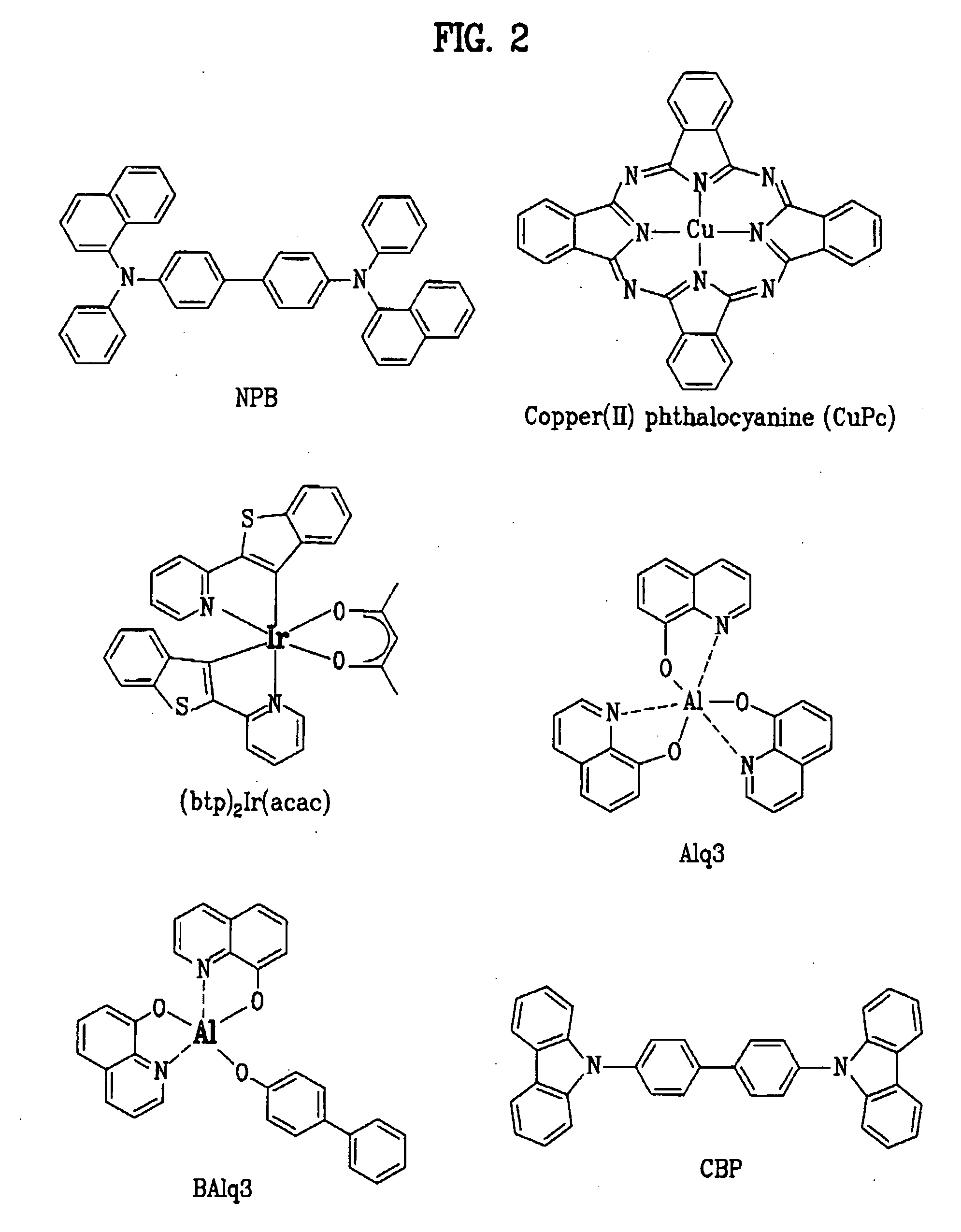
[0039] An ITO glass substrate is patterned to have a light emitting area of 3 mm×3 mm. Then, the patterned ITO glass substrate is washed. Subsequently, the substrate is mounted on a vacuum chamber. The standard pressure is set to 1×10⁻⁶ torr. Thereafter, layers of organic matter are formed on the ITO substrate in the order of CuPC (200 Å), NPB (400 Å), BAlq+A-2(7%) (200 Å), Alq3 (300 Å), LiF (5 Å), and Al (1000 Å).

[0040] At 0.9 mA, the brightness is equal to 1066 cd / m2 (6.5 V). At this point, CIE x=0.646, y=0.351. Furthermore, the durability (half of the initial brightness) lasts for 5500 hours at 2000 cd / m2.

second embodiment

2. Second Embodiment

[0041] An ITO glass substrate is patterned to have a light emitting area of 3 mm×3 mm. Then, the patterned ITO glass substrate is washed. Subsequently, the substrate is mounted on a vacuum chamber. The standard pressure is set to 1×10⁻⁶ torr. Thereafter, layers of organic matter are formed on the ITO substrate in the order of CuPC (200 Å), NPB (400 Å), BAlq+A-7(7%) (200 Å), Alq3 (300 Å), LiF (5 Å), and Al (1000 Å).

[0042] At 0.9 mA, the brightness is equal to 1102 cd / m2 (6.1 V). At this point, CIE x=0.645, y=0.352. Furthermore, the durability (half of the initial brightness) lasts for 5800 hours at 2000 cd / m2.

third embodiment

3. Third Embodiment

[0043] An ITO glass substrate is patterned to have a light emitting area of 3 mm×3 mm. Then, the patterned ITO glass substrate is washed. Subsequently, the substrate is mounted on a vacuum chamber. The standard pressure is set to 1×10⁻⁶ torr. Thereafter, layers of organic matter are formed on the ITO substrate in the order of CuPC (200 Å), NPB (400 Å), BAlq+A-9(7%) (200 Å), Alq3 (300 Å), LiF (5 Å), and Al (1000 Å).

[0044] At 0.9 mA, the brightness is equal to 949 cd / m2 (5.3 V). At this point, CIE x=0.658, y=0.339. Furthermore, the durability (half of the initial brightness) lasts for 5000 hours at 2000 cd / m2.


PUM

PropertyMeasurementUnit
Current densityaaaaaaaaaa

Abstract

Red phosphorescene compounds and organic electro-luminescence device using the same are disclosed. In an organic electroluminescence device including an anode, a hole injecting layer, a hole transport layer, a light emitting layer, an electron transport layer, an electron injecting layer, and a cathode serially deposited on one another, the organic electroluminescence device may use a compound as a dopant of the light emitting layer.

Description

[0001] This application claims the benefit of the Patent Korean Application No. 10-2005-0019181, filed on Mar. 8, 2005, which is hereby incorporated by reference as if fully set forth herein. BACKGROUND OF THE INVENTION [0002] 1. Field of the Invention [0003] The present invention relates to an organic electroluminescence device, and more particularly, to red phosphorescene compounds and organic electroluminescence device using the same. Most particularly, the present invention relates to red phosphorescence being used as a dopant of a light emitting layer of an organic electroluminescence device, which is formed by serially depositing an anode, a hole injecting layer, a hole transport layer, a light emitting layer, an electron transport layer, an electron injecting layer, and a cathode. [0004] 2. Discussion of the Related Art [0005] Recently, as the size of display devices is becoming larger, the request for flat display devices that occupy lesser space is becoming more in demand. ...

Claims


Application Information

Patent Timeline
IPC IPC(8): H01L51/54H05B33/14C09K11/06C07D215/00
CPCC07F15/0033C09K11/06C09K2211/1029C09K2211/185H01L51/0081H01L51/0085H01L51/5016H05B33/14Y10S428/917H10K85/324H10K85/342H10K50/11H10K2101/10E03D9/08
Inventor KIM, JUNG KEUNPARK, CHUN GUNSEO, JEONG DAEJEONG, HYUN CHEOLLEE, KYUNG HOONPARK, SANG TAE
Owner LG ELECTRONICS INC
Why Eureka
Try Eureka