Method of making a semiconductor interconnect with a metal cap

a metal cap and interconnect technology, applied in the field of semiconductor devices, can solve the problems of low -k insulators, low dielectric constant, and inability to provide good structural support for integration, and achieve the effect of improving the capacitive delay of chip level interconnects, low dielectric constant, and small overall effective dielectric constan

Inactive Publication Date: 2006-09-14
INFINEON TECH AG +1
View PDF25 Cites 106 Cited by
  • Summary
  • Abstract
  • Description
  • Claims
  • Application Information

AI Technical Summary

Benefits of technology

[0009] In one aspect, the present invention provides a method for forming interconnects, which is particularly useful in very small dimension devices. One way to improve the capacitive delay in the chip level interconnect is to have a smaller bulk dielectric constant in the intermetal dielectrics. In order to keep the overall effective die

Problems solved by technology

Unfortunately, as the spacing decreases, the intralevel and interlevel capacitances increase between metal lines, because the capacitance C is inversely proportional to the spacing d between the lines.
However, these low-k insulators (low compared to silicon oxide) are usually mechanically weak and some are porous and there

Method used


Image

  • Method of making a semiconductor interconnect with a metal cap
  • Method of making a semiconductor interconnect with a metal cap
  • Method of making a semiconductor interconnect with a metal cap

Examples


Embodiment Construction

[0017] The making and using of the presently preferred embodiments are discussed in detail below. It should be appreciated, however, that the present invention provides many applicable inventive concepts that can be embodied in a wide variety of specific contexts. The specific embodiments discussed are merely illustrative of specific ways to make and use the invention, and do not limit the scope of the invention.

[0018] The present invention will be described with respect to preferred embodiments in a specific context, namely a dual damascene metallization scheme. The invention may also be applied, however, to other interconnect structures. For but two examples, the process can be applied to a single damascene metallization process or to the formation of a via or contact.

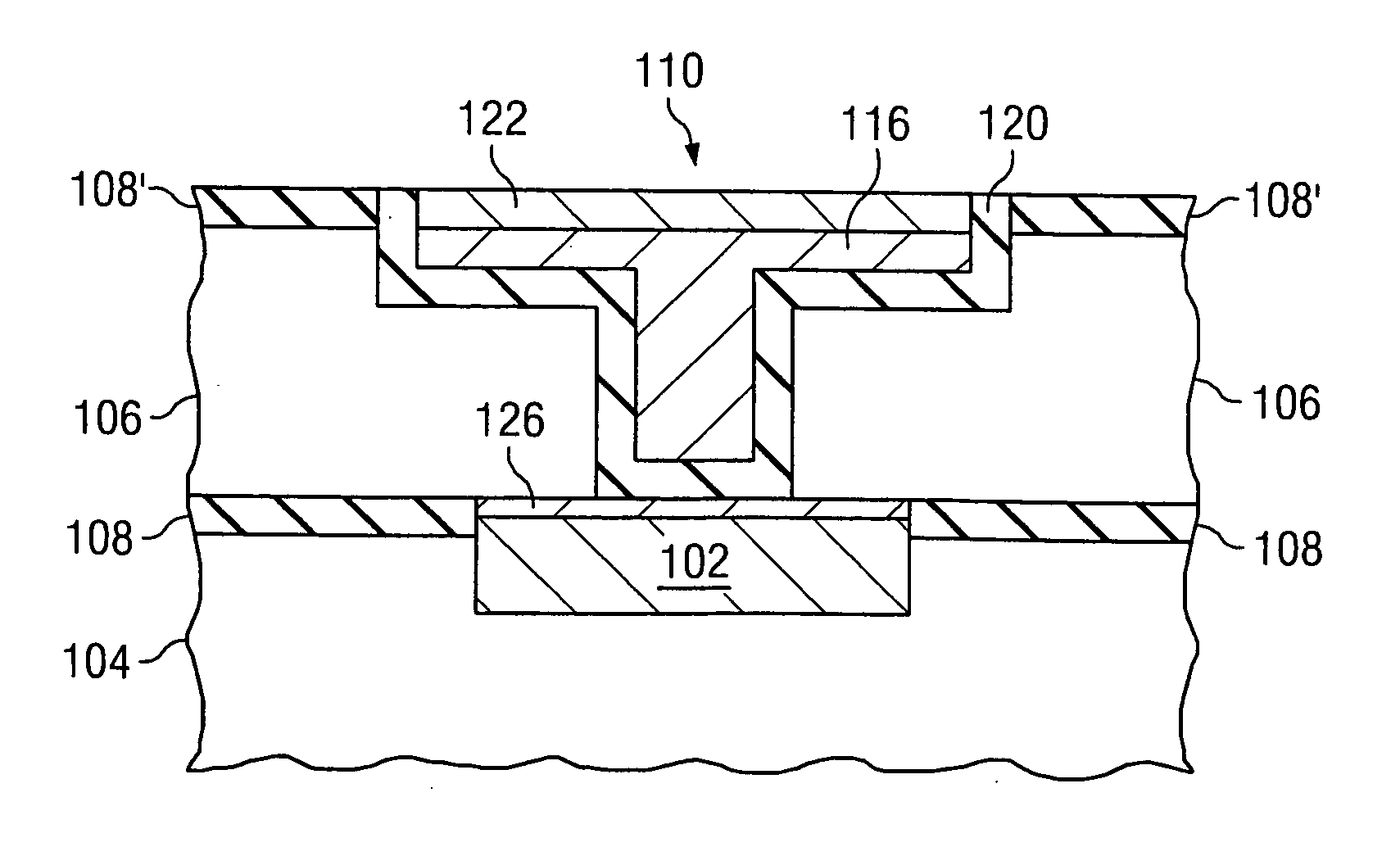
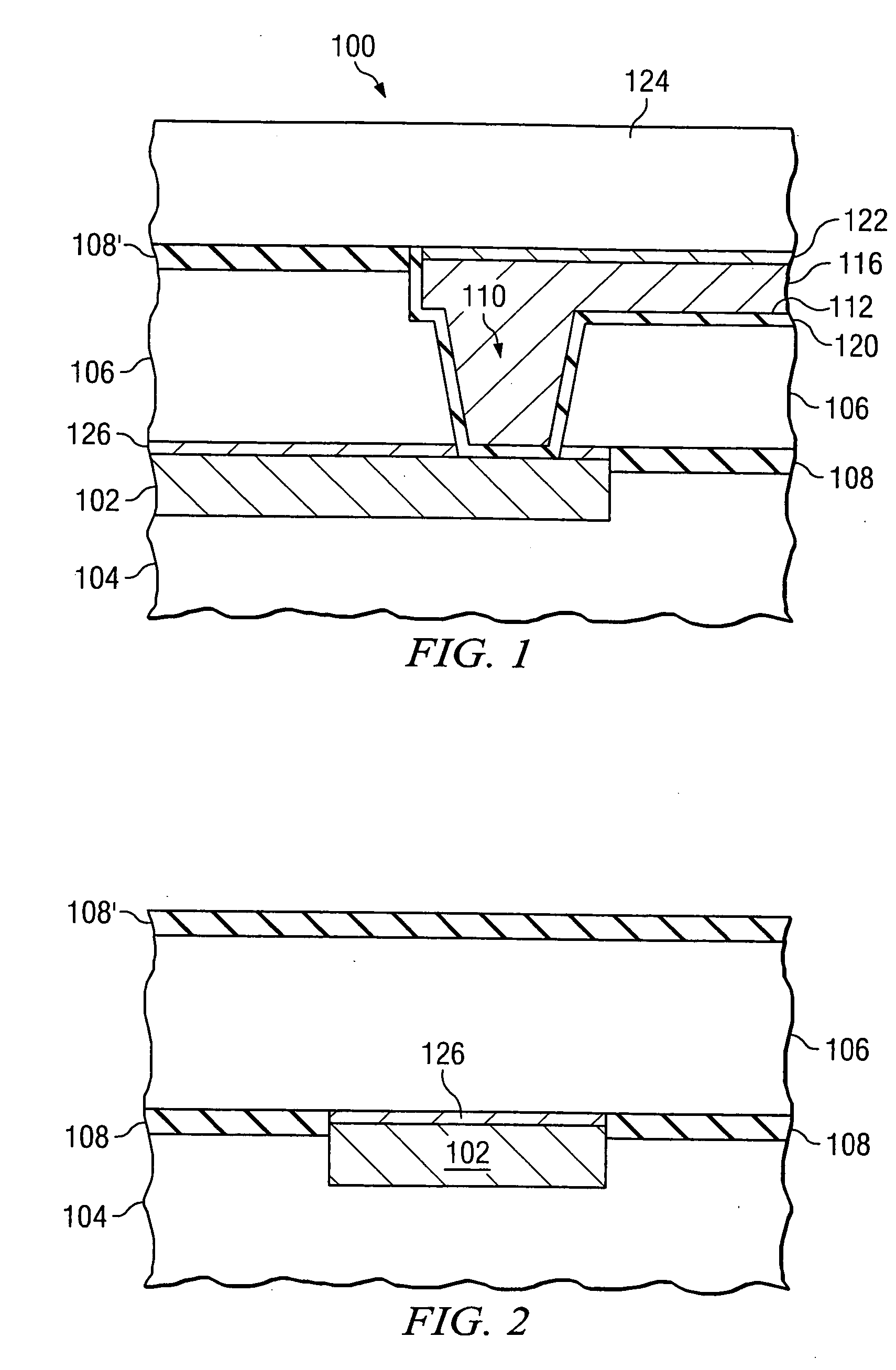
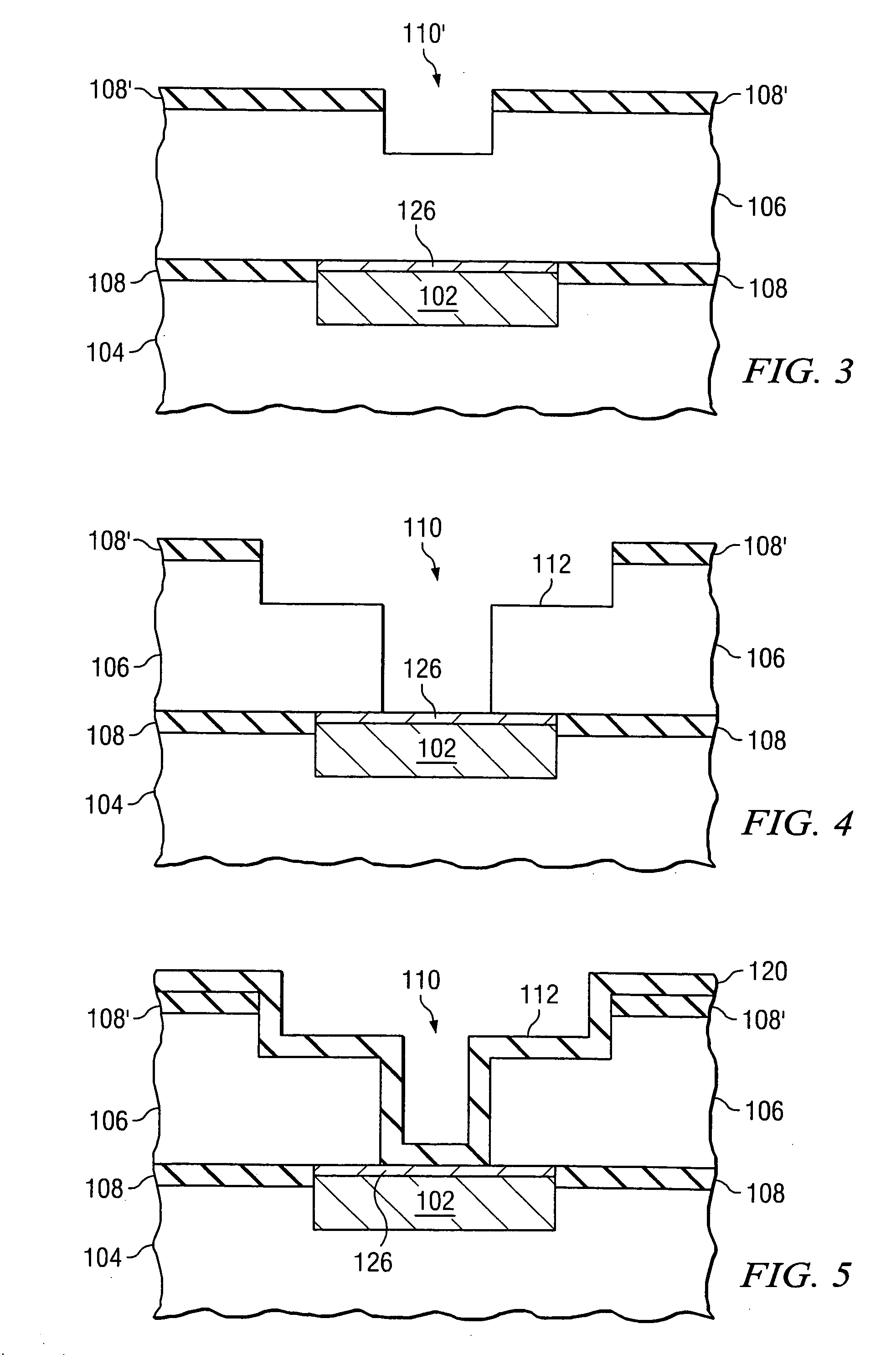
[0019] A preferred embodiment interconnect structure is illustrated in FIG. 1. One embodiment for fabricating this structure is illustrated in FIGS. 2-10. As will be explained below, and as would be understood by o...


PUM


Abstract

A method for forming metallization is particularly useful for semiconductor devices having a critical dimension of less than 160 nm. A semiconductor wafer includes an insulating layer having an upper surface. First and second trenches are formed in the insulating layer. In one embodiment, the first trench is separated from the second trench by less than 160 nm. A barrier material is formed to line the trenches and also overlies the insulating layer between the trenches. A conductive material (e.g., copper) is formed within the trenches. The conductive material is then recessed within the trenches and a metal cap layer is selectively formed over the conductive material in the trenches. The barrier material overlying the insulating layer between the first trench and the second trench is then removed. This removal will further remove any residual portions of the metal cap layer from between the first trench and the second trench.

Description

TECHNICAL FIELD [0001] This invention relates generally to semiconductor devices, and more particularly to a method of making a semiconductor interconnect with a metal cap. BACKGROUND [0002] As Ultra Large Scale Integration (ULSI) circuit density increases and device feature sizes approach 0.18 microns or less, increased numbers of patterned metal levels are required with decreasing spacing between metal lines at each level to effectively interconnect discrete semiconductor devices on the semiconductor chips. Typically, the different levels of metal interconnections are separated by layers of insulator material. These interposed insulating layers have etched holes filled with a conductive material, referred to as vias, which are used to connect one level of metal to the next. Typically, the insulating layer is silicon oxide (SiO2) having a dielectric constant k (relative to vacuum) of about 4.0 or 4.5. [0003] However, as semiconductor device dimensions decrease and the packing densi...

Claims


Application Information

Patent Timeline
IPC IPC(8): H01L21/4763
CPCH01L21/7684H01L21/76843H01L21/76849H01L21/76873
Inventor BECK, MICHAEL
Owner INFINEON TECH AG
Why Eureka
Try Eureka