Stacked spacer structure and process

Inactive Publication Date: 2004-12-07
WINBOND ELECTRONICS CORP
View PDF7 Cites 8 Cited by
  • Summary
  • Abstract
  • Description
  • Claims
  • Application Information

AI Technical Summary

Benefits of technology

The stacked spacer structure of the present invention can shrink the width of the stacked spacer and

Problems solved by technology

Unfortunately, one problem occurs because much thinner oxide sidewall spacers are used to achieve the higher device density.
A cleaning step is used to remove any native oxide left on the substrate, and the thin oxide sidewall spacers are attacked resulting in electrical shorts between the SAC plug and gate electrode.
Although the nitride sidewall spacer can

Method used


Image

  • Stacked spacer structure and process
  • Stacked spacer structure and process
  • Stacked spacer structure and process

Examples


Embodiment Construction

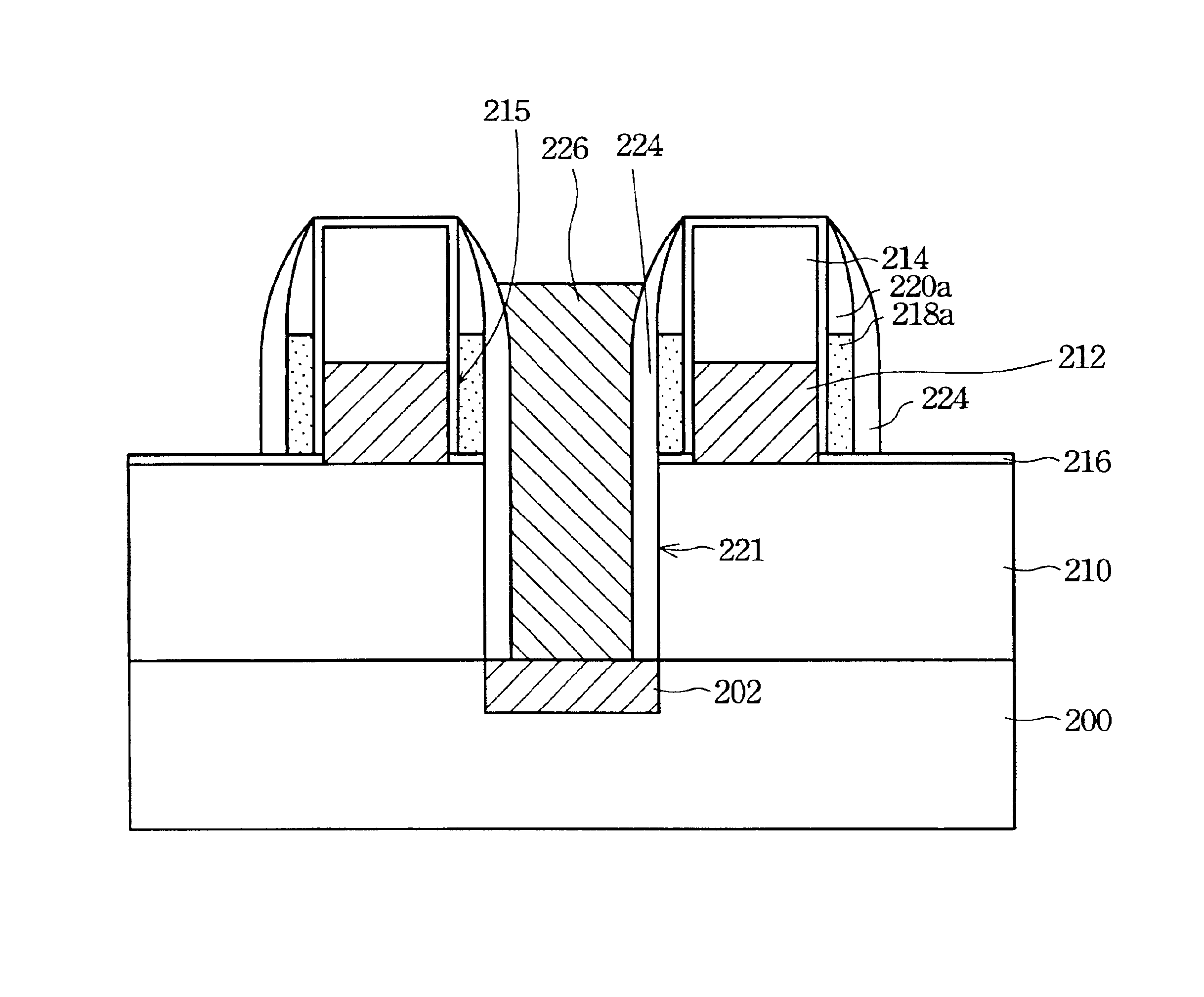
The present invention provides a stacked spacer structure in which a low dielectric bottom portion is formed under a silicon nitride top portion and a silicon nitride outer portion covered thereon to reduce the equivalent dielectric constant. Furthermore, by precisely controlling and shrinking the width of the stacked spacer structure, device dimension is reduced and thus the integrated density is improved.

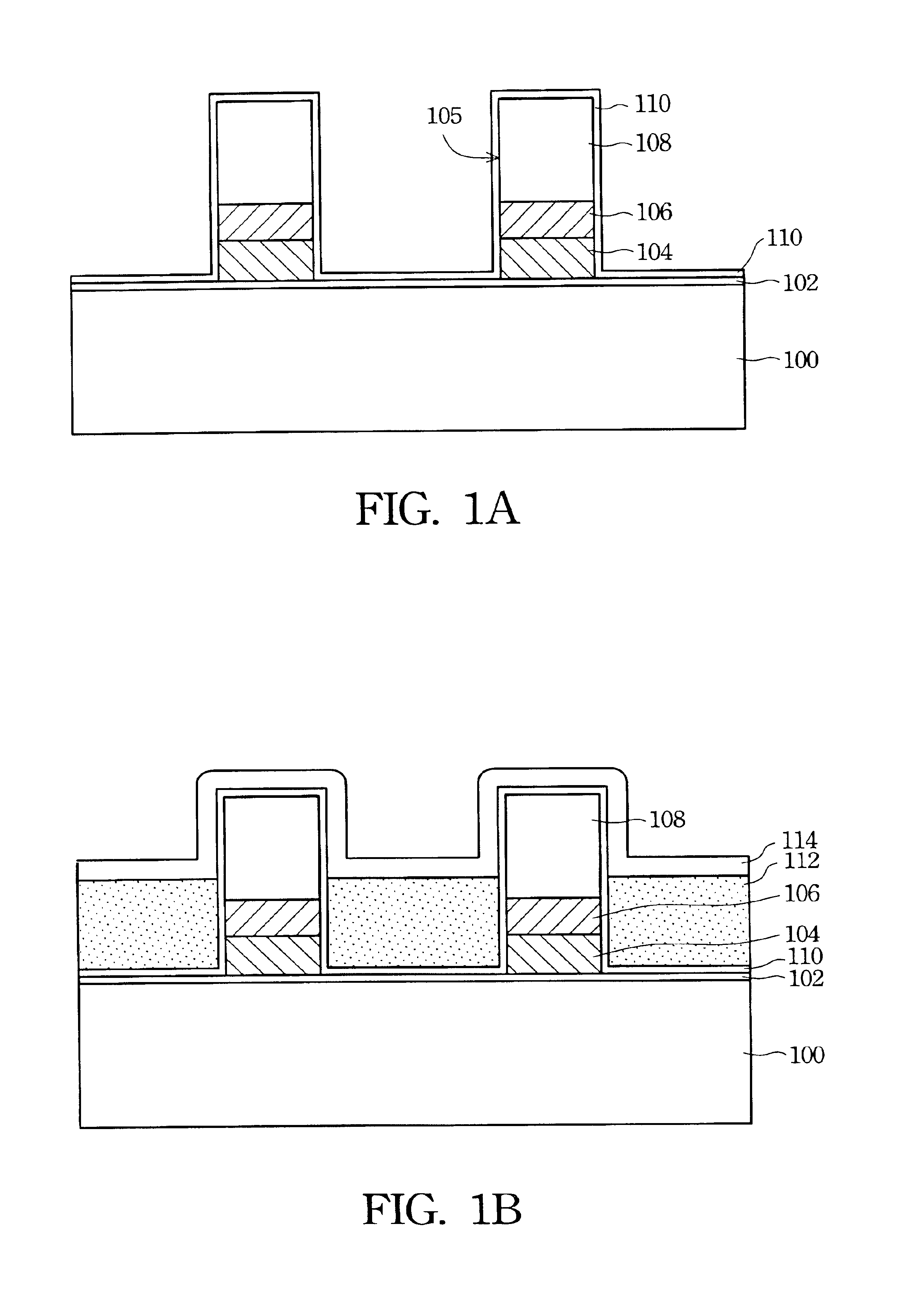
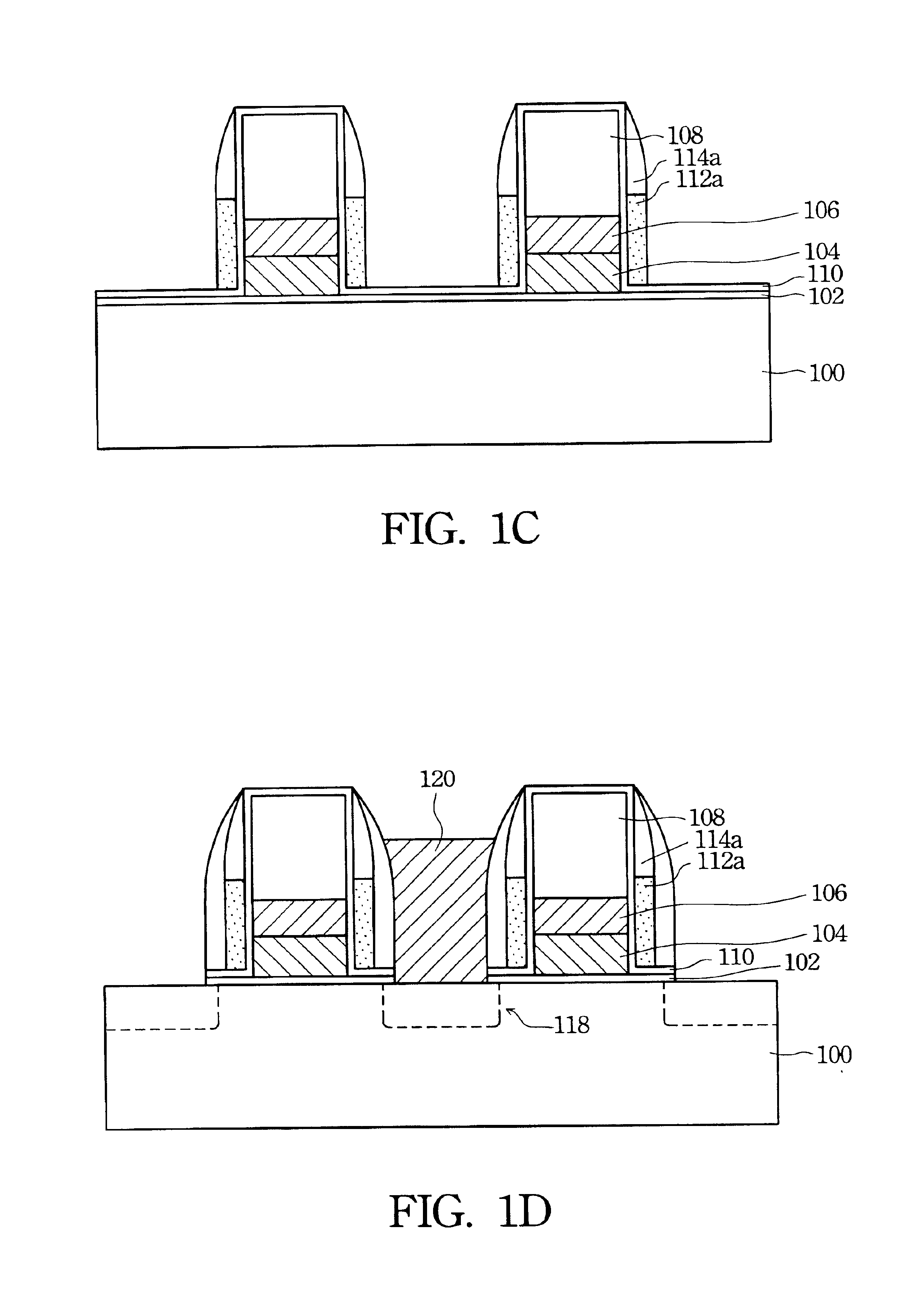
FIGS. 1A-1D are schematic, cross-sectional views according to one preferred embodiment of the claimed invention. Referring to FIG. 1A, a semiconductor substrate 100 such as a silicon substrate with a lattice orientation is provided. A stacked gate layer, e.g., a word line or a branch connecting to the word line, is formed on an active area (not shown) of the substrate 100 after completing device isolation. The stacked gate layer comprises a gate dielectric layer, a gate conductive layer and a gate cap layer, stacked from bottom to top, respectively. The gate dielectric layer can ...


PUM


Abstract

A stacked spacer structure and process adapted for a stacked layer on a semiconductor substrate is described. The stacked spacer structure is formed on the sidewalls of the stacked layer which comprise a conductive layer and a cap layer thereon. A dielectric layer made of a material with low dielectric constant lower than that of silicon nitride is formed on the semiconductor substrate. A first silicon nitride layer is then formed over the substrate. The first silicon nitride layer and dielectric layer are etched sequentially to form an inner spacer on the sidewalls of the stacked layer. A second silicon nitride layer is formed over the substrate and is etched to form an outer spacer on the sidewalls of the inner spacer. By forming the stacked spacer structure of the present invention embedded in low dielectric material, the coupling capacitance produced therein will be greatly reduced.

Description

FIELD OF THE INVENTIONThe present invention relates to a semiconductor device structure and to the process for forming the structure, and more particularly to a stacked spacer structure and process for its formation, which can effectively reduce coupling capacitance.BACKGROUND OF THE INVENTIONThe computer and the electronic industry consistently demand of increased overall speed as well as lower fabrication costs for integrated circuits. As far as a computer is concerned, doubtlessly, the integrated circuits, such as Dynamic Random Access Memory (DRAM), play a crucial role. A great number of DRAM memory cells are usually required, and thus they are a vital factor for determining the I / O speed of the computer. Hence, pursuing the miniaturization of the DRAM devices so as to lower costs as well as attain a high-speed performance is one major goal in the industry.The miniaturization of devices according to a scaling rule is used in a semiconductor device to achieve large-scale integrat...

Claims


Application Information

Patent Timeline
IPC IPC(8): H01L21/60H01L29/417H01L21/02H01L21/70H01L21/336H01L21/8242H01L29/40H01L21/311H01L21/318H01L21/316
CPCH01L21/31116H01L21/76897H01L27/10855H01L29/66636H01L29/41766H01L29/6656H01L21/31612H01L21/3185H01L27/10888H01L27/10891H01L27/10885H10B12/488H10B12/485H10B12/0335H10B12/482H01L21/02164H01L21/0217
Inventor YANG, SHIH-HSIENCHUANG, YUEH-CHENGSHEU, BOR-RU
Owner WINBOND ELECTRONICS CORP
Why Eureka
Try Eureka