
Eureka
For R&D, Eureka makes reading and utilizing patents & technical documents easy.
Eureka AIR
Designed for self-driven R&D workflows. Generate viable solutions, solve complex R&D challenges, empower your innovation with AI.

Eureka Materials
Designed for material experts only. Revolutionize your material R&D, from search, analyze, to developing new materials.

TechResearch
Generate reliable direction feasibility study reports for your R&D in just a few steps.

TechSeek
Discover and master advanced knowledge NOW. Basics, ideas, possibilities, all at once.

TechMind
As an expert in R&D Theories, TechMind can generates customized viable solutions instantly.

TechRisk
Analyze your overall solution with one click, know your potential R&D risks in advance.

TechMonitor
Get weekly tech updates, stay abreast of the latest tech innovations and key insights.
DC offset cancel control method and transmitter/receiver
- Summary
- Abstract
- Description
- Claims
- Application Information
AI Technical Summary
Benefits of technology
Problems solved by technology
Method used
Image

Examples
Embodiment Construction
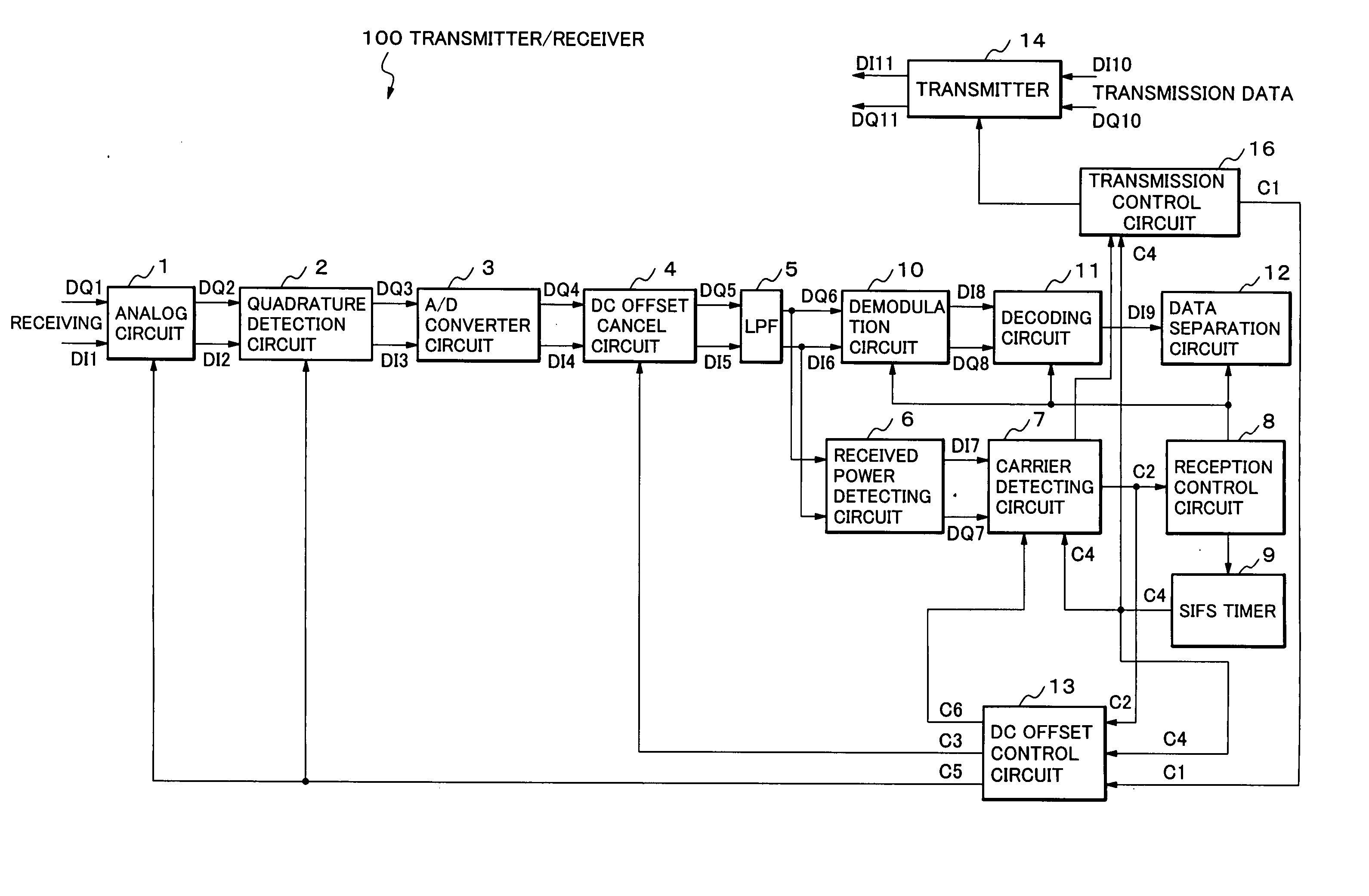
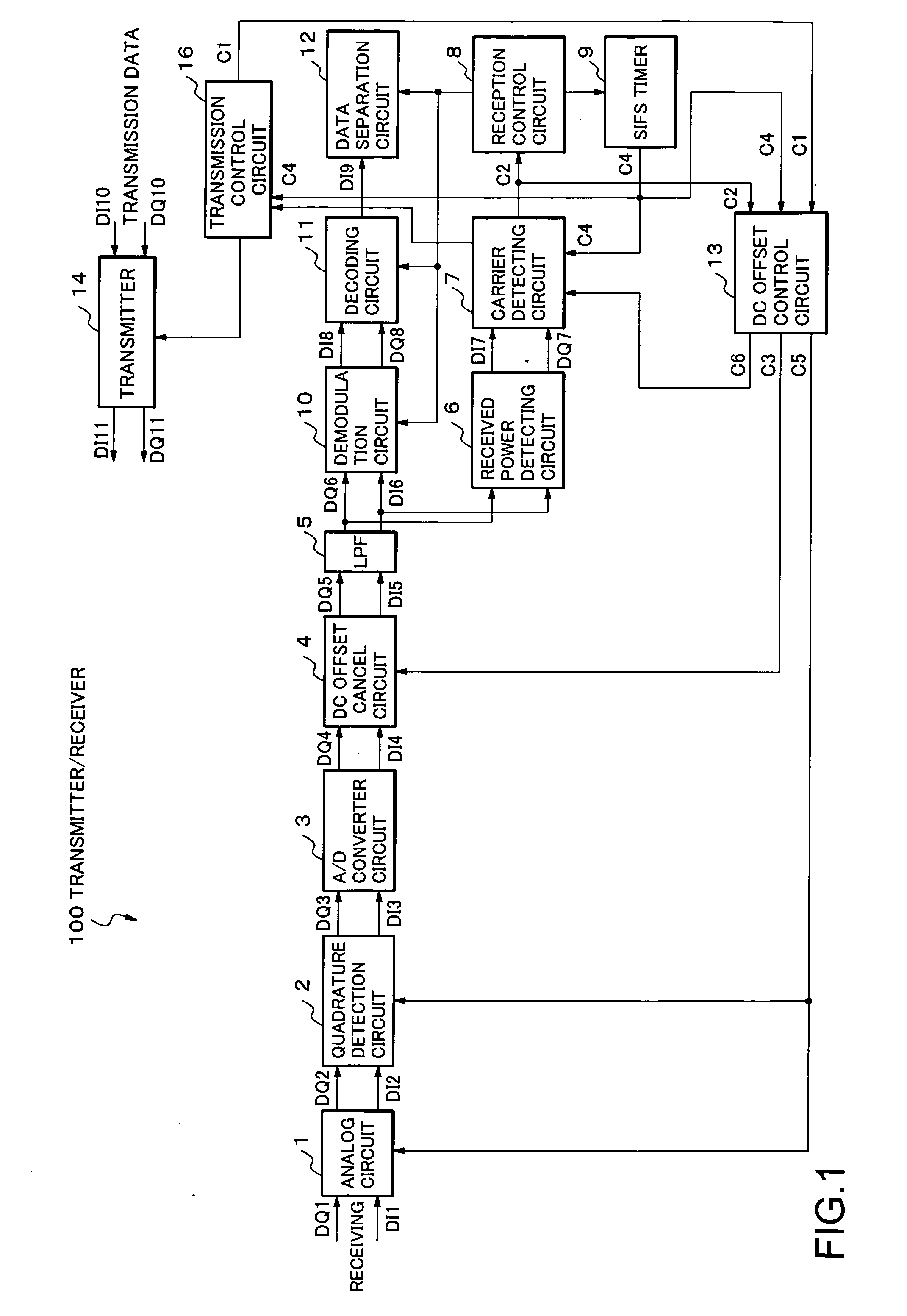
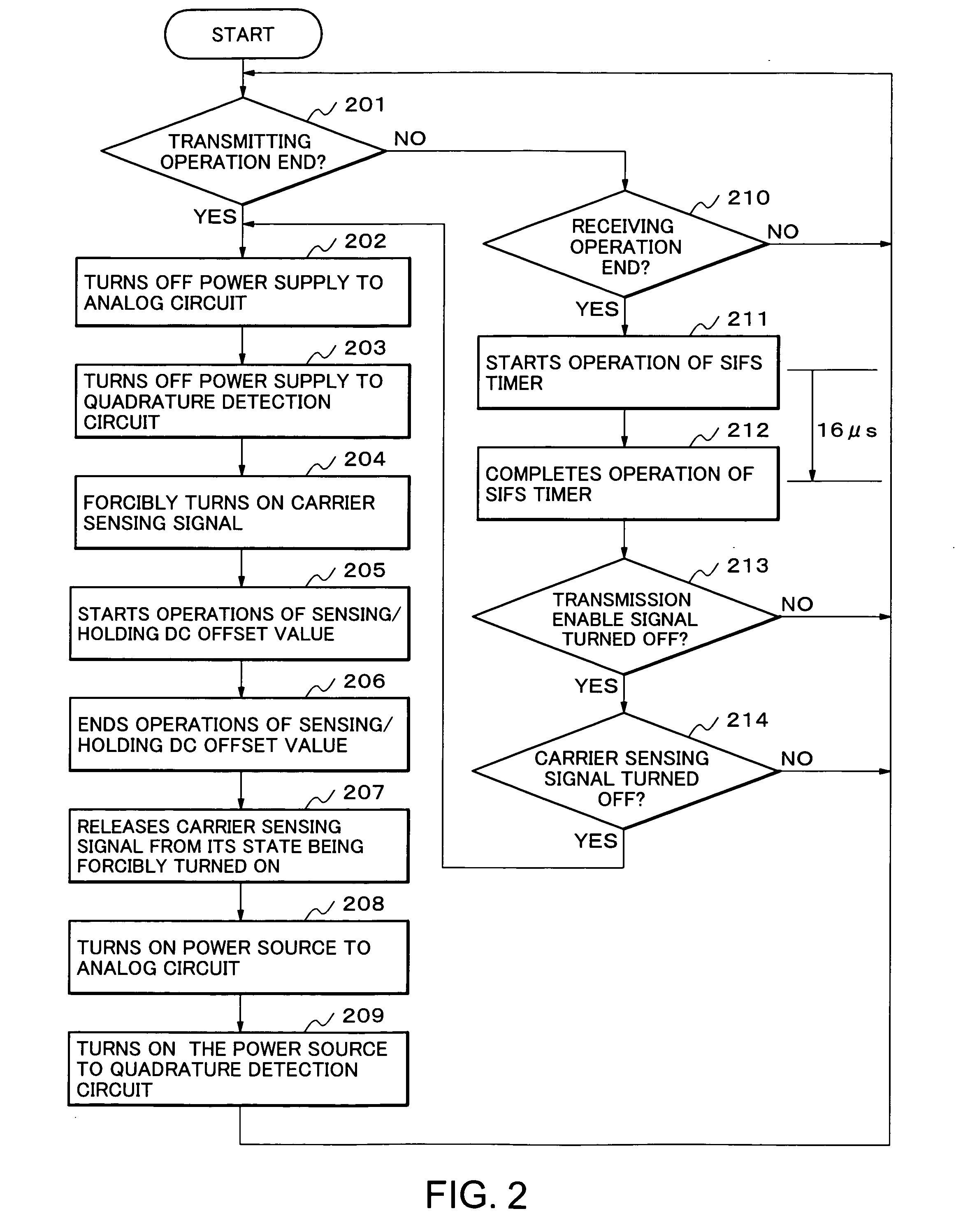
[0021] Hereinafter, exemplary embodiments of present invention will be described in detail with reference to the accompanying drawings. FIG. 1 is a block diagram showing a configuration example of a transmitter / receiver to which a DC offset canceling control method according to the present invention is applied. This example is a transmitter / receiver in a packet switching system using CSMA / CA.
[0022] This transmitter / receiver 100 includes an analog circuit 1, a quadrature detection circuit 2, an A / D converter 3, a DC offset cancel circuit 4, a low-pass filter (LPF) 5, a received power detecting circuit 6, a carrier detection circuit 7, a reception control circuit 8, an SIFS timer 9, a demodulation circuit 10, a decoding circuit 11, a data separation circuit 12, a DC offset control circuit 13, a transmitter 14, and a transmission control circuit 16.
[0023] The transmitter / receiver 100 of FIG. 1 is characterized by including the DC offset cancel circuit 4 and the DC offset control circ...
PUM
 Abstract
Description
Claims
Application Information
 - R&D Engineer
- R&D Manager
- IP Professional
- Industry Leading Data Capabilities
- Powerful AI technology
- Patent DNA Extraction
Browse by: Latest US Patents, China's latest patents, Technical Efficacy Thesaurus, Application Domain, Technology Topic, Popular Technical Reports.
© 2024 PatSnap. All rights reserved.Legal|Privacy policy|Modern Slavery Act Transparency Statement|Sitemap|About US| Contact US: help@patsnap.com