Wireless functional testing of RFID tag

Active Publication Date: 2006-09-14
IMPINJ
View PDF40 Cites 36 Cited by
  • Summary
  • Abstract
  • Description
  • Claims
  • Application Information

AI Technical Summary

Problems solved by technology

Therefore RFID tag solutions tend to be sensitive to production and/or implementation costs.
Another RFID tag cost structure issue concerns the packaging of the RFID tag die.
If the RFID tag chips from a same wafer are not sufficiently functional

Method used


Image

  • Wireless functional testing of RFID tag
  • Wireless functional testing of RFID tag
  • Wireless functional testing of RFID tag

Examples


Embodiment Construction

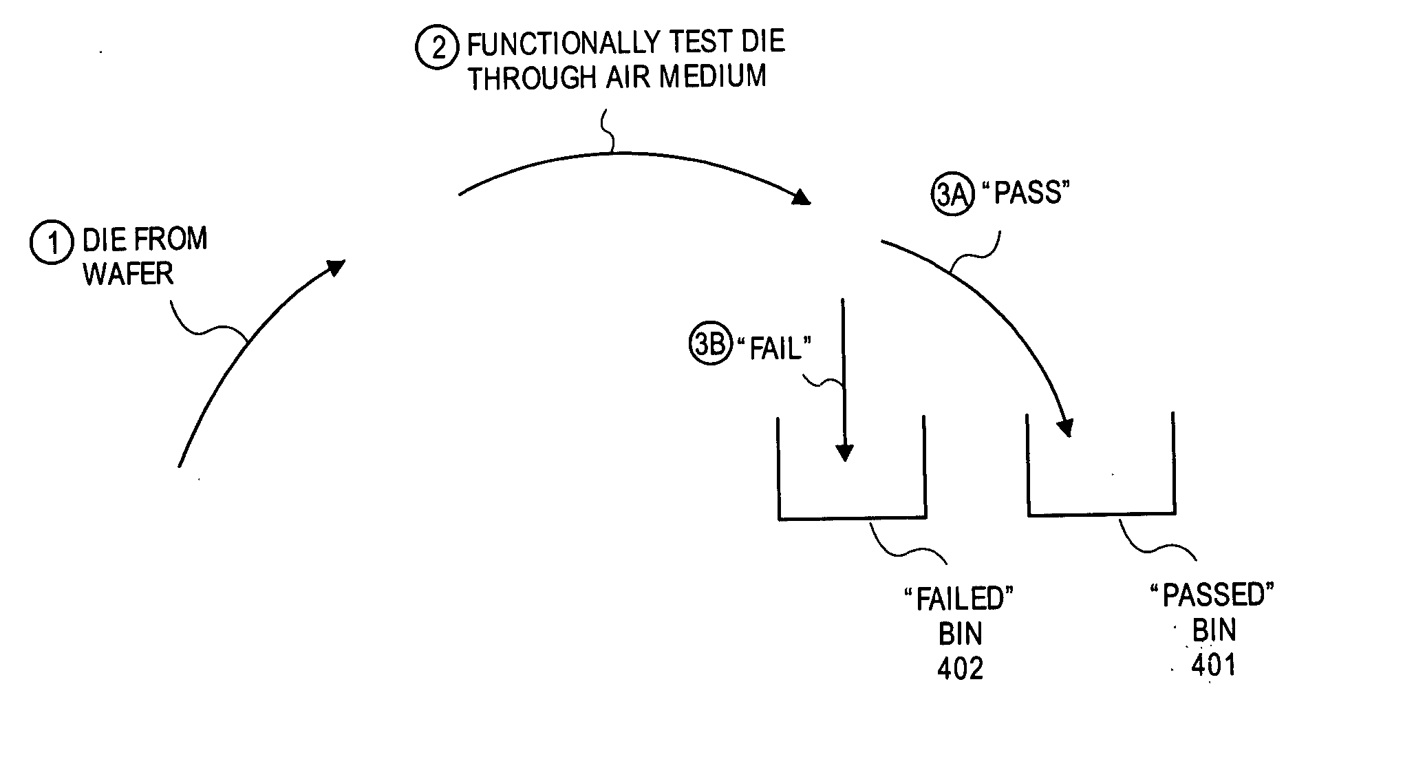
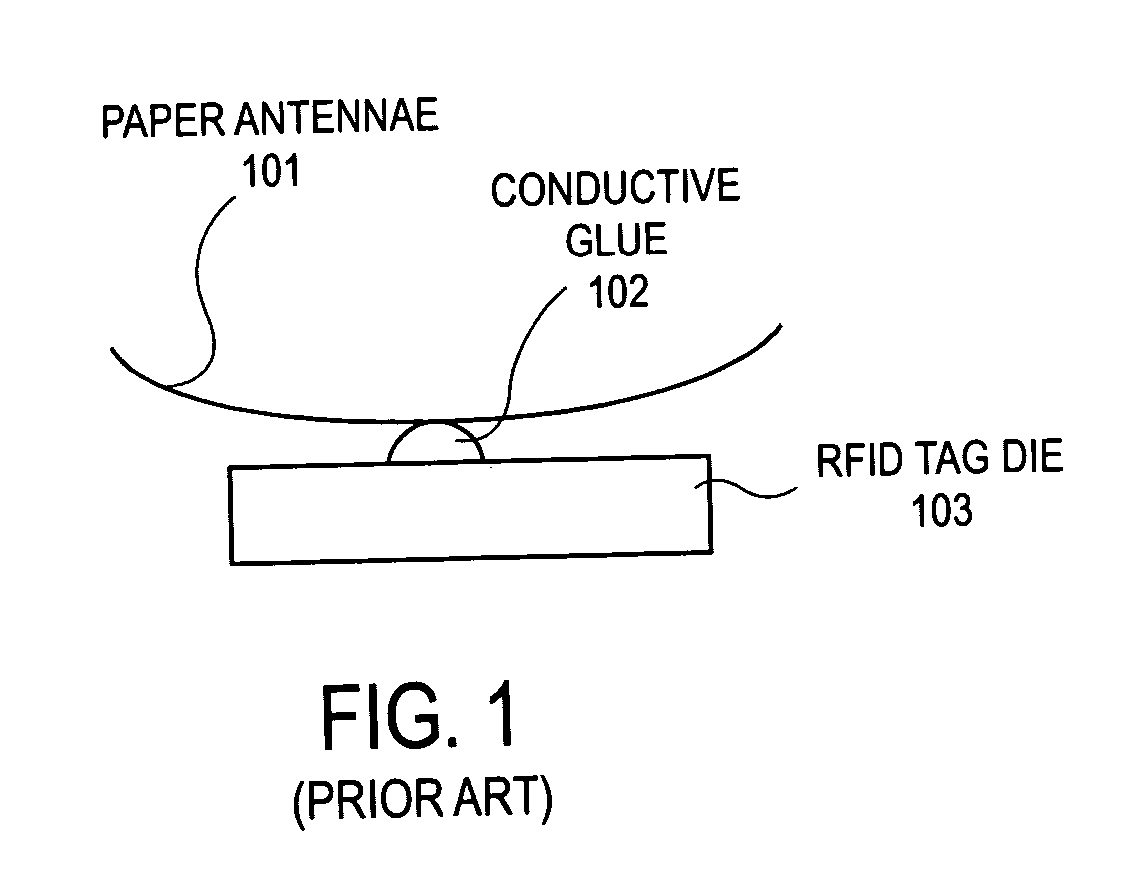
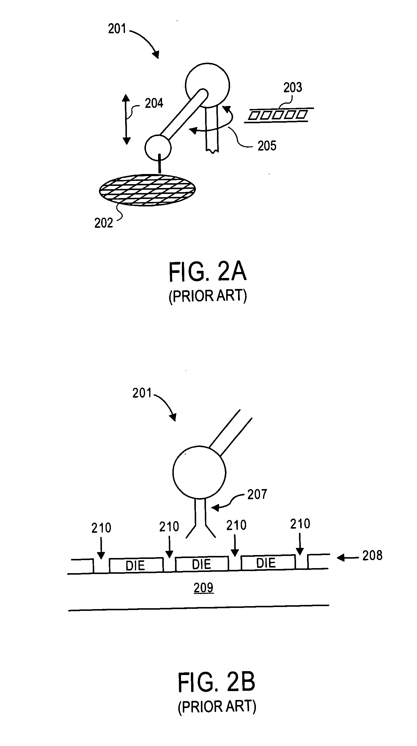
[0035] Recalling from the description in the Background that prior art RFID tags have not been designed with integrated “on die” antenna (because the size of the antenna is not large enough to detect signals from distant readers); and, that functional testing of an RFID tag prior to its packaging would help reduce the manufactured cost of an RFID tag die (because a “bad” die could be identified before expending the cost of its packaging); then, a solution is to design an RFID tag with an integrated “on die” antenna for purposes of functionally testing the die prior to its packaging. Here, an “on-die” antenna is an antenna that is part of the integrated circuitry of the RFID tag formed with the semiconductor manufacturing process used to manufacture the RFID tag itself.

[0036] Moreover, certain types of business and / or technology models may involve the shipment of working die that have not been packaged into a discrete “per die” packages (e.g., a ceramic casing having leads or other ...


PUM

PropertyMeasurementUnit
Structureaaaaaaaaaa
Areaaaaaaaaaaa
Metallic bondaaaaaaaaaa

Abstract

Wirelessly testing an RFID tag before it is packaged or otherwise entered into a process reserved for “working” RFID tags is described. Various processes that employ such wireless testing as well as various “on-die” RFID tag antennae designs for facilitating the wireless testing are also described.

Description

FIELD OF THE INVENTION [0001] The field of invention relates to the semiconductor chip arts; and, more specifically, to the functional testing of an RFID tag BACKGROUND OF THE INVENTION RFID Tags [0002] A Radio Frequency Identification (RFID) tag is a semiconductor chip (also referred to as a “die” or integrated circuit) that can positively respond to a wireless signal sent by a “reader” that inquires into the RFID tag's existence. By positively responding to the reader's wireless signal, the RFID tag can verify its presence to the reader. Frequently cited RFID tag applications include automated inventory management systems and automated transportation / distribution systems (e.g., a pallet affixed with an RFID tag will be able to wirelessly identify itself to an intelligent warehousing reader system so as to confirm its presence within the warehouse). [0003] The less expensive an RFID tag solution, the easier it is to justify the expense of integrating RFID tag semiconductor chips a...

Claims


Application Information

Patent Timeline
IPC IPC(8): G01N37/00G08B13/14B07C5/344G01R31/28G01R31/302G01R31/01
CPCB07C5/344G01R31/01Y10T29/49004H01L2223/6677G01R31/2822
Inventor HORCH, ANDREW E.
Owner IMPINJ
Why Eureka
Try Eureka