Supercharge Your Innovation With Domain-Expert AI Agents!

Electrical fuse for silicon-on-insulator devices

a technology of silicon-on-insulator and electric fuse, which is applied in the direction of semiconductor devices, semiconductor/solid-state device details, electrical apparatus, etc., can solve the problems of affecting the efficiency of the laser, the use of the laser, and the use of complex processing steps. achieve the effect of efficient and cost-effectiv

Inactive Publication Date: 2006-09-21
WU CHI HSI
View PDF13 Cites 13 Cited by
  • Summary
  • Abstract
  • Description
  • Claims
  • Application Information

AI Technical Summary

Benefits of technology

This approach enables the efficient and cost-effective incorporation of electrical fuses into SOI devices, allowing for customization and redundancy without adding process complexity or cost, by forming the fuse simultaneously with other semiconductor devices like transistors.

Problems solved by technology

If a memory circuit is found to be defective or is not needed, the fuse may be blown by activating or deactivating the redundant memory cells.
The use of the laser, however, requires complicated processing steps and expensive laser equipment.

Method used


Image

  • Electrical fuse for silicon-on-insulator devices
  • Electrical fuse for silicon-on-insulator devices
  • Electrical fuse for silicon-on-insulator devices

Examples


Embodiment Construction

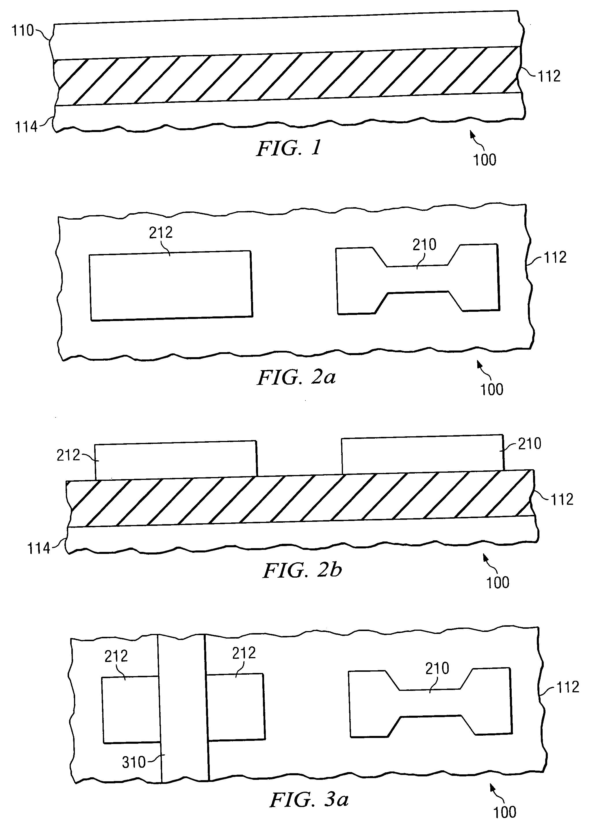
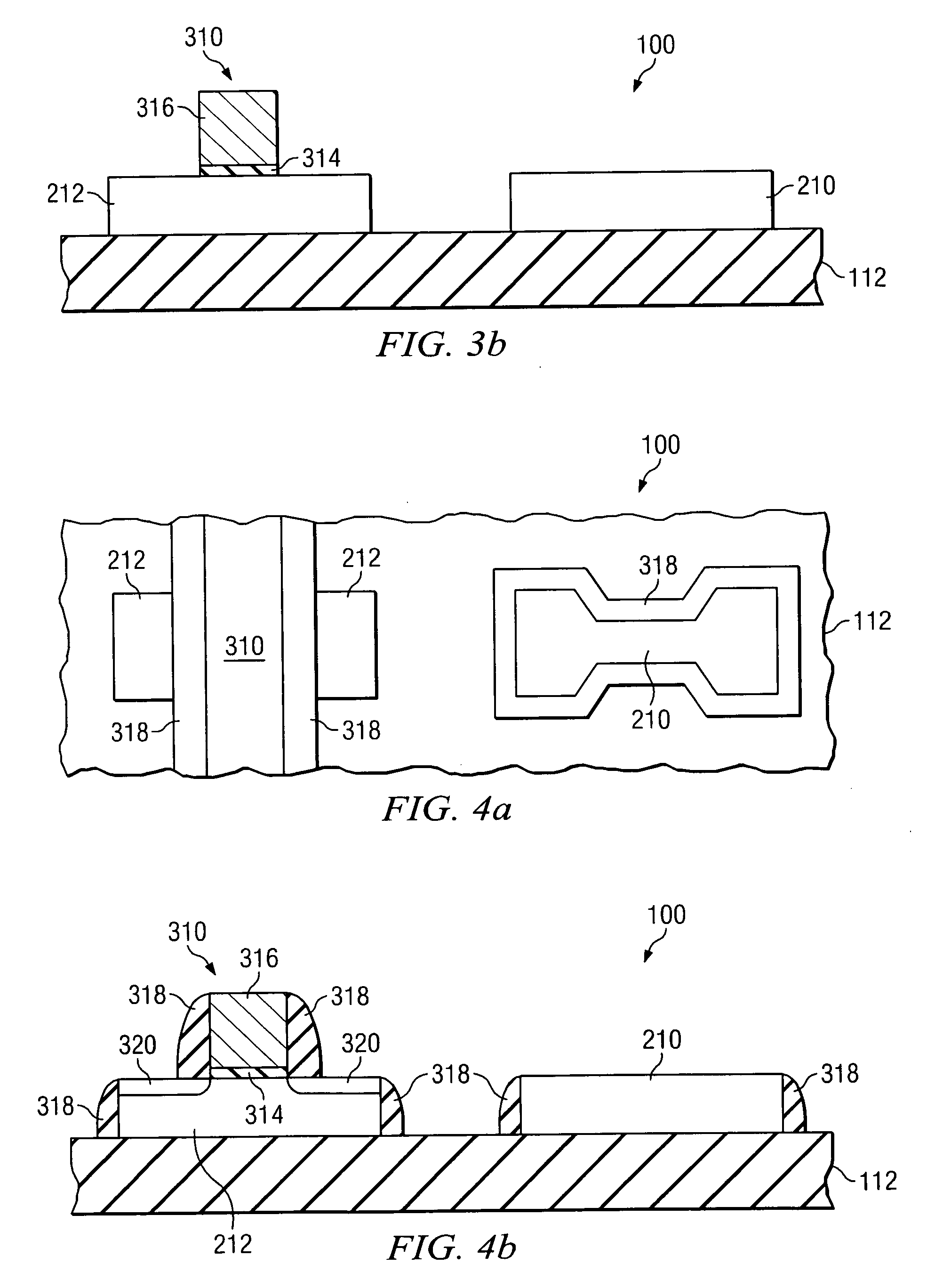
[0016] The making and using of the presently preferred embodiments are discussed in detail below. It should be appreciated, however, that the present invention provides many applicable inventive concepts that can be embodied in a wide variety of specific contexts. The specific embodiments discussed are merely illustrative of specific ways to make and use the invention, and do not limit the scope of the invention.

[0017] Referring now to the drawings, wherein like reference numerals are used herein to designate like elements throughout the various views, preferred embodiments of the present invention are illustrated and described. As will be understood by one of ordinary skill in the art, the figures are not necessarily drawn to scale, and in some instances the drawings have been exaggerated and / or simplified in places for illustrative purposes only. One of ordinary skill in the art will appreciate the many applications and variations of the present invention in light of the followin...


PUM


Abstract

An apparatus for providing an electrical fuse is provided. An electrical fuse is patterned from the active layer of a semiconductor-on-insulator (SOI) wafer. One shape of the electrical fuse may be a first and second portion electrically coupled via a third section. The third section is typically thinner than the first and second portion. An ion implant is performed to fully deplete the electrical fuse, and a silicidation process is performed. Thereafter, standard processing techniques may be used to form vias and other integrated circuit structures.

Description

[0001] This application is a divisional of patent application Ser. No. 10 / 811,405, entitled “Method of Fabricating an Electrical Fuse for Silicon-On-Insulator Devices,” filed on Mar. 26, 2006, which application is incorporated herein by reference.TECHNICAL FIELD [0002] The present invention relates to semiconductor devices and, in particular, to an electrical fuse for silicon-on-insulator devices. BACKGROUND [0003] Fuses are commonly used in integrated circuits to provide redundancy and programming capabilities. To increase yield in integrated circuits such as memory chips, it is common to include redundant memory cells on the memory chips. If a memory circuit is found to be defective or is not needed, the fuse may be blown by activating or deactivating the redundant memory cells. Another common practice is to utilize fuses to program or customize integrated circuits for a particular application or customer. In this manner, the same chip may be produced and customized for individual...

Claims


Application Information

Patent Timeline
Patent Type & Authority Applications(United States)
IPC IPC(8): H01L21/82H01L21/00H01L21/84H01L23/525H01L23/62H01L27/12H01L27/13
CPCH01L21/84H01L23/5256H01L29/785H01L27/13H01L27/1203H01L2924/0002H01L2924/00
Inventor WU, CHI-HSI
Owner WU CHI HSI
Features
  • R&D
  • Intellectual Property
  • Life Sciences
  • Materials
  • Tech Scout
  • Unparalleled Data Quality
  • Higher Quality Content
  • 60% Fewer Hallucinations
Learn More