Posted write buffers and method of posting write requests in memory modules

a write buffer and memory module technology, applied in the field of computer systems, can solve the problems of slow memory controller and memory device speed, limiting data bandwidth between the processor and the memory device, and increasing the operating speed of the processor,

Inactive Publication Date: 2006-09-21
ROUND ROCK RES LLC
View PDF99 Cites 32 Cited by
  • Summary
  • Abstract
  • Description
  • Claims
  • Application Information

AI Technical Summary

Problems solved by technology

Although the operating speed of memory devices has continuously increased, this increase in operating speed has not kept pace with increases in the operating speed of processors.
The relatively slow speed of memory controllers and memory devices limits the data bandwidth between the processor and the memory devices.
In addition to the limited bandwidth between processors and system memory devices, the performance of computer systems is also limited by latency problems that increase the time required to read data from system memory devices.
Therefore, although SDRAM devices can synchronously output burst data at a high data rate, the delay in initially providing the data can significantly slow the operating speed of a computer system using such SDRAM devices as system memory.
Memory read latency may also be adversely impacted by the need to write data to memory devices.
More specifically, if a controller issues a write request followed by a read request, it may not be possible for a memory device to which the requests are issued to respond to the read request until after the write request has been serviced.
Therefore, write requests can considerably increase memory read latencies.
Although the use of posted write buffers provides significant advantages in conventional computer systems, it is likely to be less advantageous in a computer system having a memory system using a hub architecture.
A posted write buffer located in the controller is likely to be inadequate in handling the vastly higher rate of write requests that would be directed to several memory modules each of which includes a memory hub coupled to several memory devices.
Not only is the bandwidth that the posted write buffer would be required to handle vastly greater with a hub architecture, but the difficulty in ensuring write buffer coherency is also vaster greater.
The large amount of write requests that would need to be buffered with a hub architecture in a system having a large number of memory addresses would make it very difficult to ensure coherency in conventional posted write buffers.

Method used


Image

  • Posted write buffers and method of posting write requests in memory modules
  • Posted write buffers and method of posting write requests in memory modules
  • Posted write buffers and method of posting write requests in memory modules

Examples


Embodiment Construction

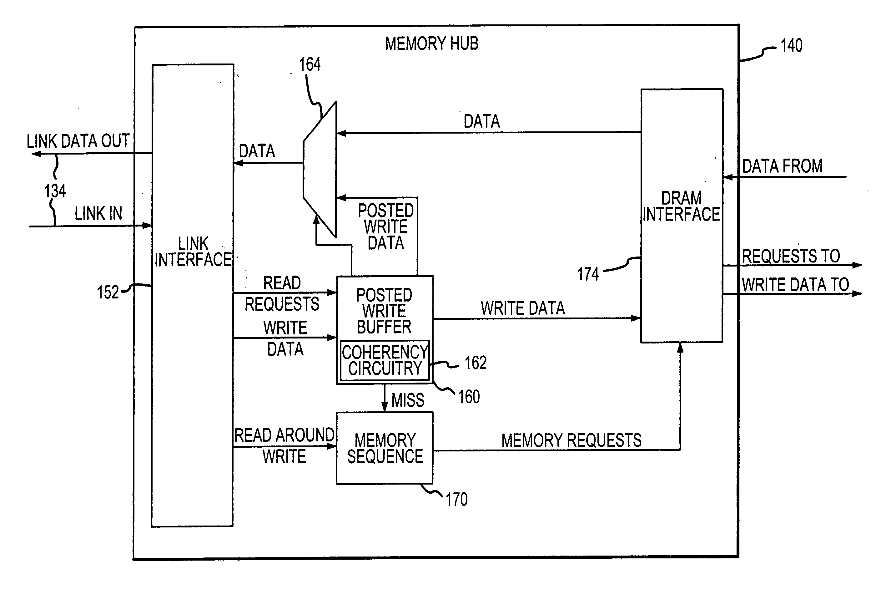
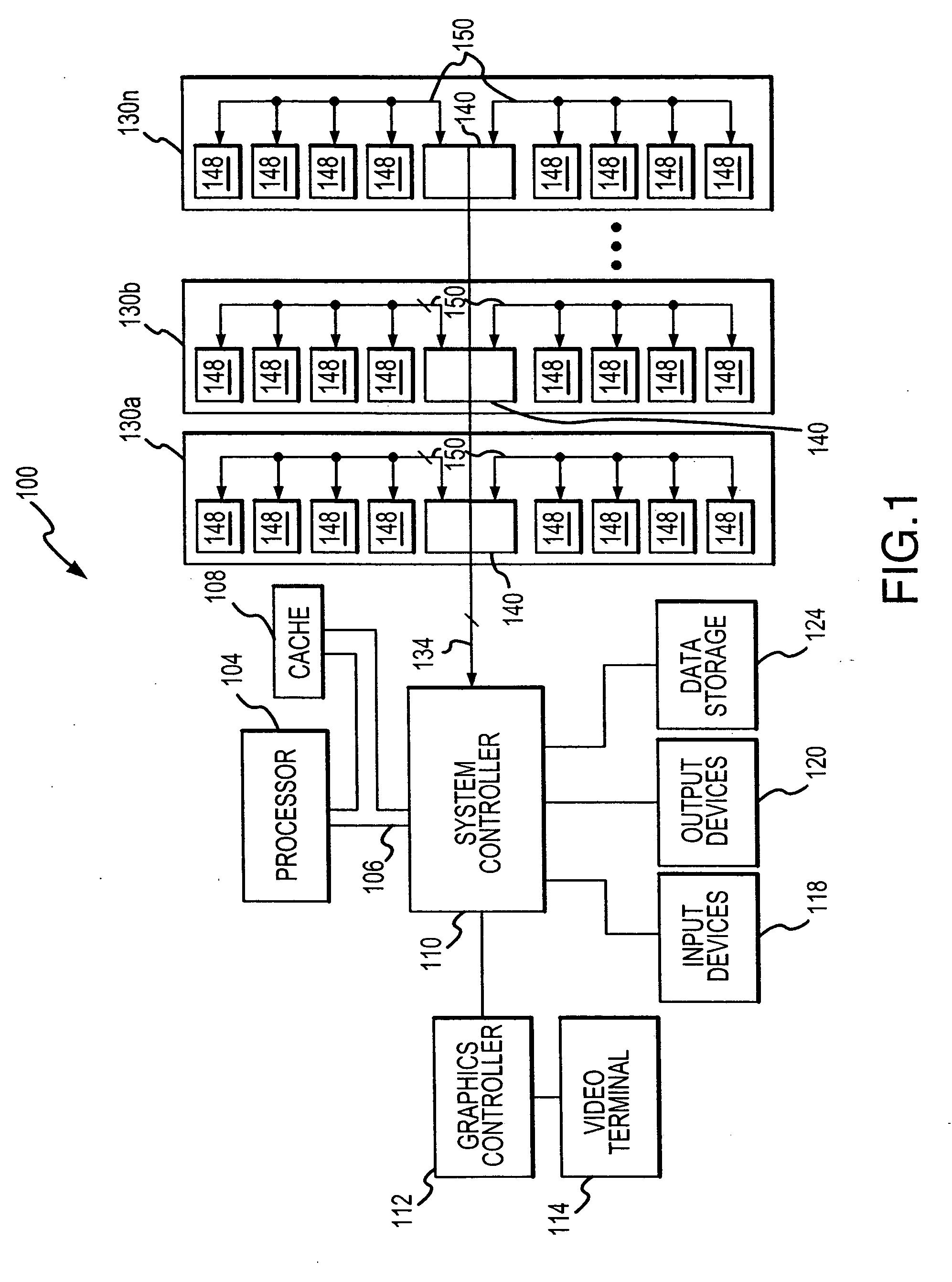
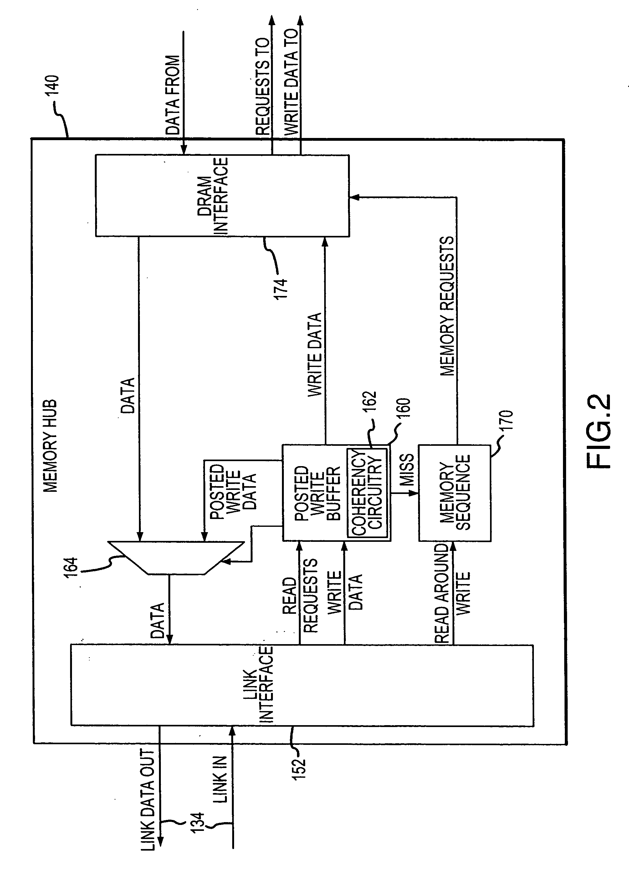
[0014] A computer system 100 according to one example of the invention is shown in FIG. 1. The computer system 100 includes a processor 104 for performing various computing functions, such as executing specific software to perform specific calculations or tasks. The processor 104 includes a processor bus 106 that normally includes an address bus, a control bus, and a data bus. The processor bus 106 is typically coupled to cache memory 108, which, as previously mentioned, is usually static random access memory (“SRAM”). Finally, the processor bus 106 is coupled to a system controller 110, which is also sometimes referred to as a “North Bridge” or “memory controller.”

[0015] The system controller 110 serves as a communications path to the processor 104 for a variety of other components. More specifically, the system controller 110 includes a graphics port that is typically coupled to a graphics controller 112, which is, in turn, coupled to a video terminal 114. The system controller 11...


PUM


Abstract

A memory module includes a memory hub coupled to several memory devices. The memory hub includes a posted write buffer that stores write requests so that subsequently issued read requests can first be coupled to the memory devices. The write request addresses are also posted in the buffer and compared to subsequent read request addresses. In the event of a positive comparison indicating that a read request is directed to an address to which an earlier write request was directed, the read data are provided from the buffer. When the memory devices are not busy servicing read request, the write requests can be transferred from the posted write buffer to the memory devices. The write requests may also be accumulated in the posted write buffer until either a predetermined number of write requests have been accumulated or the write requests have been posted for a predetermined duration.

Description

TECHNICAL FIELD [0001] This invention relates to computer systems, and, more particularly, to a computer system having a processor or other memory access device coupled to a plurality of memory modules each of which includes a memory hub coupled to a plurality of memory devices. BACKGROUND OF THE INVENTION [0002] Computer systems use memory devices, such as dynamic random access memory (“DRAM”) devices, to store data that are accessed by a processor. These memory devices are normally used as system memory in a computer system. In a typical computer system, the processor communicates with the system memory through a processor bus and a memory controller. The processor issues a memory request, which includes a memory command, such as a read command, and an address designating the location from which data or instructions are to be read. The memory controller uses the command and address to generate appropriate command signals as well as row and column addresses, which are applied to th...

Claims


Application Information

Patent Timeline
Patent Type & Authority Applications(United States)
IPC IPC(8): G06F12/00G11C7/10G11C11/4093G11C11/4096
CPCG11C7/1006G11C7/1051G11C7/1069G11C7/1078G11C7/1096G11C11/4093G11C11/4096
Inventor JEDDELOH, JOSEPH M.LEE, TERRY R.
Owner ROUND ROCK RES LLC
Why Eureka
Try Eureka