Semiconductor device and method of controlling said semiconductor device

Active Publication Date: 2006-09-28
VALLEY DEVICE MANAGEMENT
View PDF11 Cites 1 Cited by
  • Summary
  • Abstract
  • Description
  • Claims
  • Application Information

AI Technical Summary

Benefits of technology

[0014] A more specific object of the present invention is to provide a semiconductor device that can protect memory cells from false rewrite without an increase in chip size, and a method of controlling the semiconductor device.
[0029] As described so far, the present invention provides a semiconductor device that can protect memory cell groups from rewrite, without an increase in chip size, and a method of controlling the semiconductor device.

Problems solved by technology

However, a NAND flash memory does not have a protecting function for each block like a NOR flash memory.
Because of this, there is a problem that data might be rewritten in accordance with a false rewrite instruction sent from the outside.

Method used


Image

  • Semiconductor device and method of controlling said semiconductor device
  • Semiconductor device and method of controlling said semiconductor device
  • Semiconductor device and method of controlling said semiconductor device

Examples


first embodiment

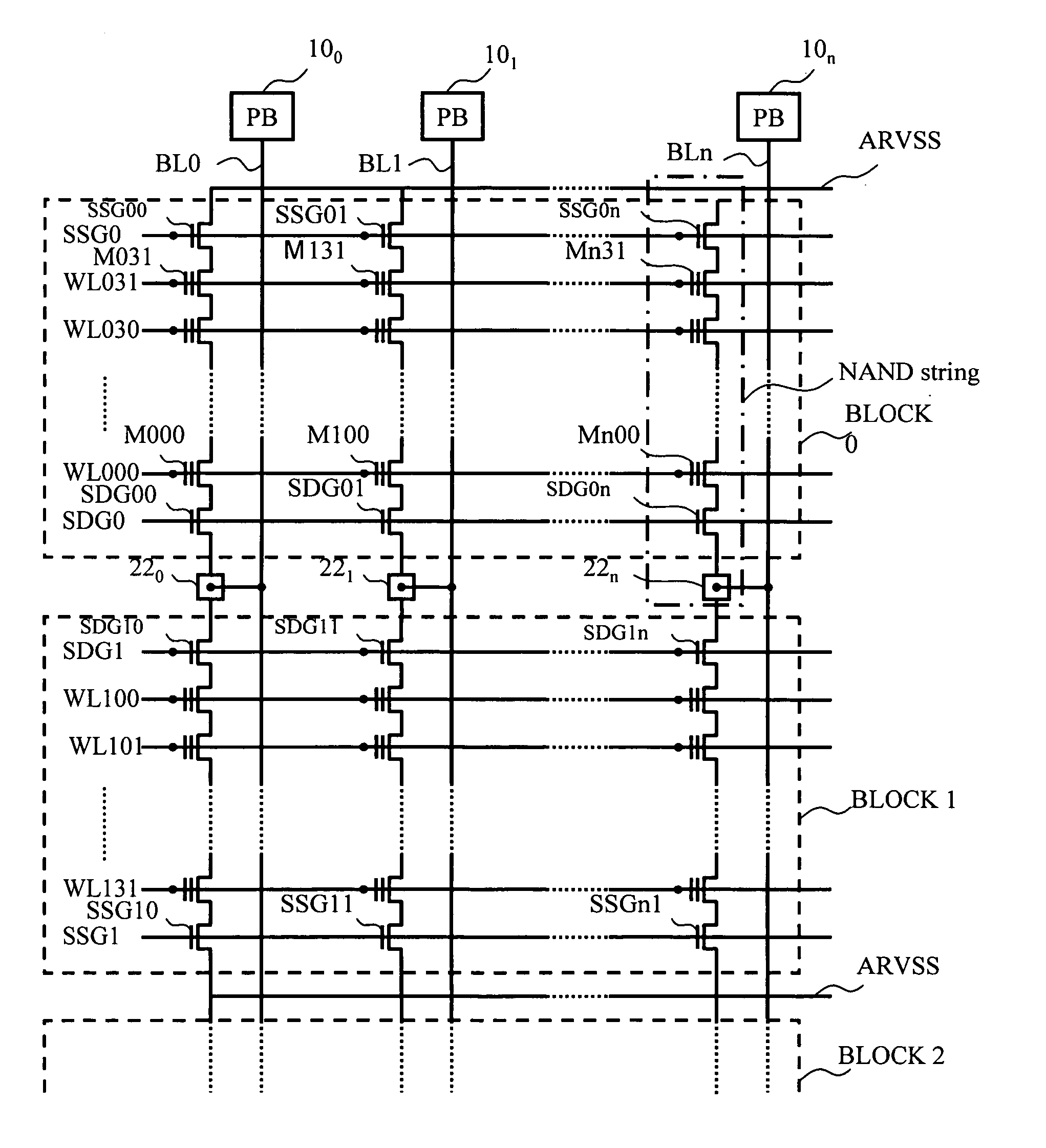
[0049]FIG. 3 is a block diagram of a NAND flash memory in accordance with the first embodiment. A flash memory 51 includes a memory cell array 52, an I / O register and buffer 53, an address register 54, a status register 55, a command register 56, a state machine 57, a high-voltage generating circuit 58, a row decoder 59, a page buffer 60, and a column decoder 61.

[0050] In the memory cell array 52, rewritable non-volatile memory cell transistors are arranged in line with word lines WL and bit lines BL that are arranged in a matrix fashion.

[0051] The I / O register and buffer 53 controls various signals or data corresponding to I / O terminals. The address register 54 temporarily stores address signals that are input through the I / O register and buffer 53. The status register 55 temporarily stores status information. The command register 56 temporarily stores operation commands that are input through the I / O register and buffer.

[0052] The state machine 57 controls the operation of each...

second embodiment

[0083] Next, a second embodiment of the present invention is described. FIG. 14 illustrates a SONOS-type NAND flash memory array and the program voltage conditions in the second embodiment. FIG. 15 is a timing chart with respect to the voltage conditions for program verification and programming in the second embodiment. Table 4 shows the conditions for program verification and programming in a selected block.

TABLE 4Sel WLUnsel WLCWLSSGARVSSBLPre-chargeVpgmvVpassVpassVssVss1 V(3 V)(6 V)(6 V)PGM Verify senseVpgmvVpassVpassVpassVsssensed(3 V)(6 V)(6 V)(6 V)PGMVppVpass_pgmVpgm_cwlVssVssVcc / Vss(20 V)(10 V)2.5 V

[0084] The loading of write data from the outside is the same as that in the first embodiment, and therefore, only the differences between the first embodiment and the second embodiment are described below. In a program verifying period, a voltage of 6V that is the same as the voltage normally applied at the time of reading is applied as Vpass to the control word lines CWL at the...


PUM


Abstract

A semiconductor device includes: groups of memory cells that are connected to word lines; and select gates that are controlled by control word lines and are connected to the groups of memory cells, each of the select gates being capable of storing protection information for a respective one of the groups of memory cells.

Description

CROSS REFERENCE TO RELATED APPLICATIONS [0001] This is a continuation of International Application No. PCT / JP2004 / 017807 filed Nov. 30, 2004. BACKGROUND OF THE INVENTION [0002] 1. Field of the invention [0003] The present invention relates to semiconductor devices and methods of controlling the semiconductor devices, and more particularly, to a semiconductor device that has a protecting function against rewrite, and a method of controlling the semiconductor device. [0004] 2. Description of the Related Art [0005] As flash memories for storing data, NAND-type memories and AND-type memories are well known. Japanese Unexamined Patent Publication No. 2001-308209 and Japanese Laid-Open Patent Publication No. 2001-518696 disclose examples of NAND flash memories that have floating gates (FG) as charge accumulation layers. [0006]FIG. 1 illustrates the array structure of a conventional FG-type NAND flash memory. In FIG. 1, WL000 through WL031 are word lines that are provided for each unit blo...

Claims


Application Information

Patent Timeline
IPC IPC(8): G11C16/04
CPCG11C16/0466G11C16/0483G11C16/22G11C16/3459
Inventor YANO, MASARUAOKI, MINORU
Owner VALLEY DEVICE MANAGEMENT
Why Eureka
Try Eureka