

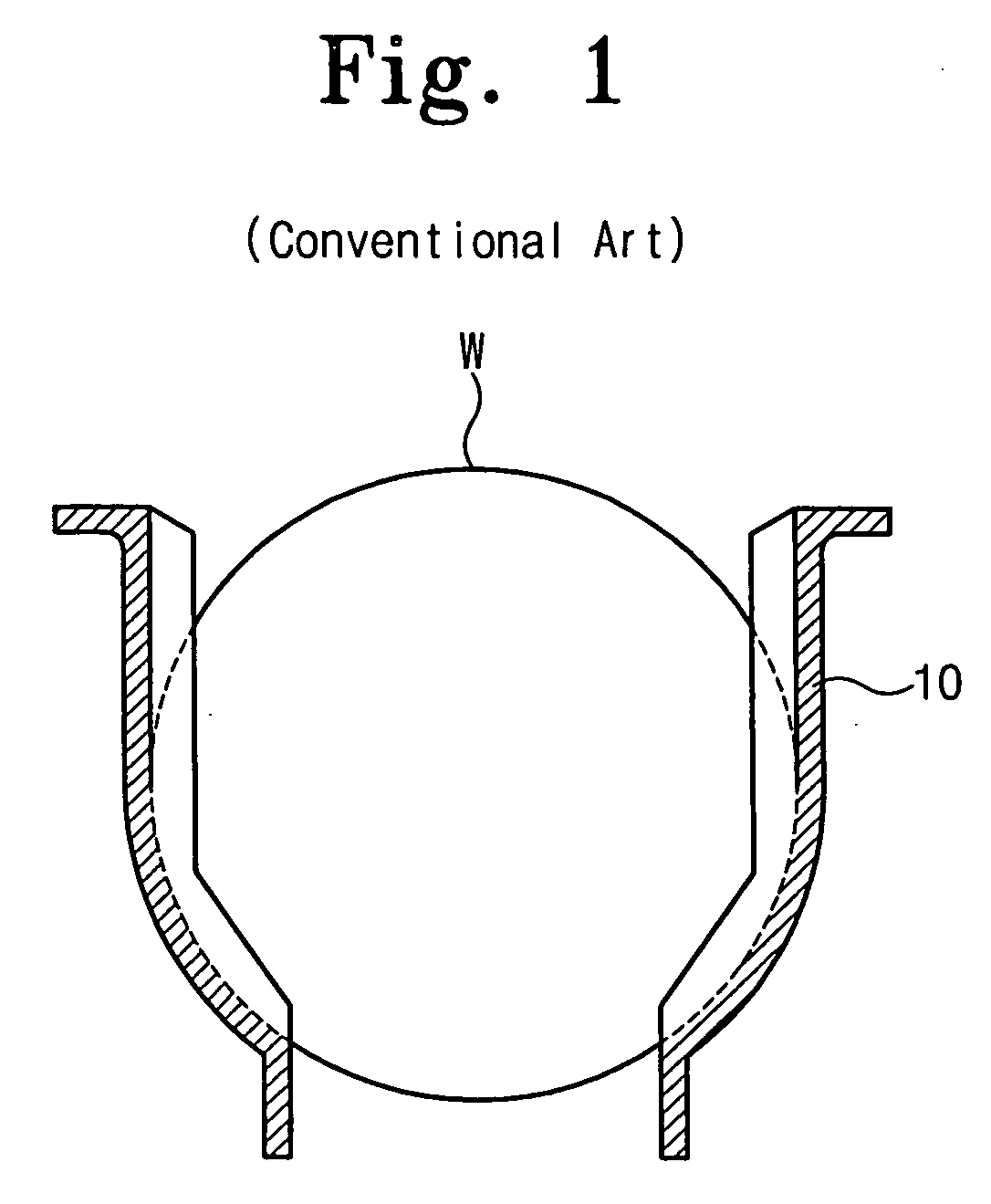
Wafer carrier for minimizing contacting area with wafers
a technology of reducing the contact area and wafers, which is applied in the direction of transportation and packaging, packaging foodstuffs, and packaged goods types, etc. it can solve the problems of reducing the washing effectiveness of the wafer, affecting and affecting the overall surface of the wafer, so as to reduce the direct contact area, reduce the occurrence of contact-induced foreign particles, and improve the overall surface. the effect of the washing effect of the wafer's
- Summary
- Abstract
- Description
- Claims
- Application Information
AI Technical Summary
Benefits of technology
Problems solved by technology
Method used
Image

Examples
Embodiment Construction
[0030] Reference will now be made in detail to the exemplary embodiments of the present invention, examples of which are illustrated in the accompanying drawings.
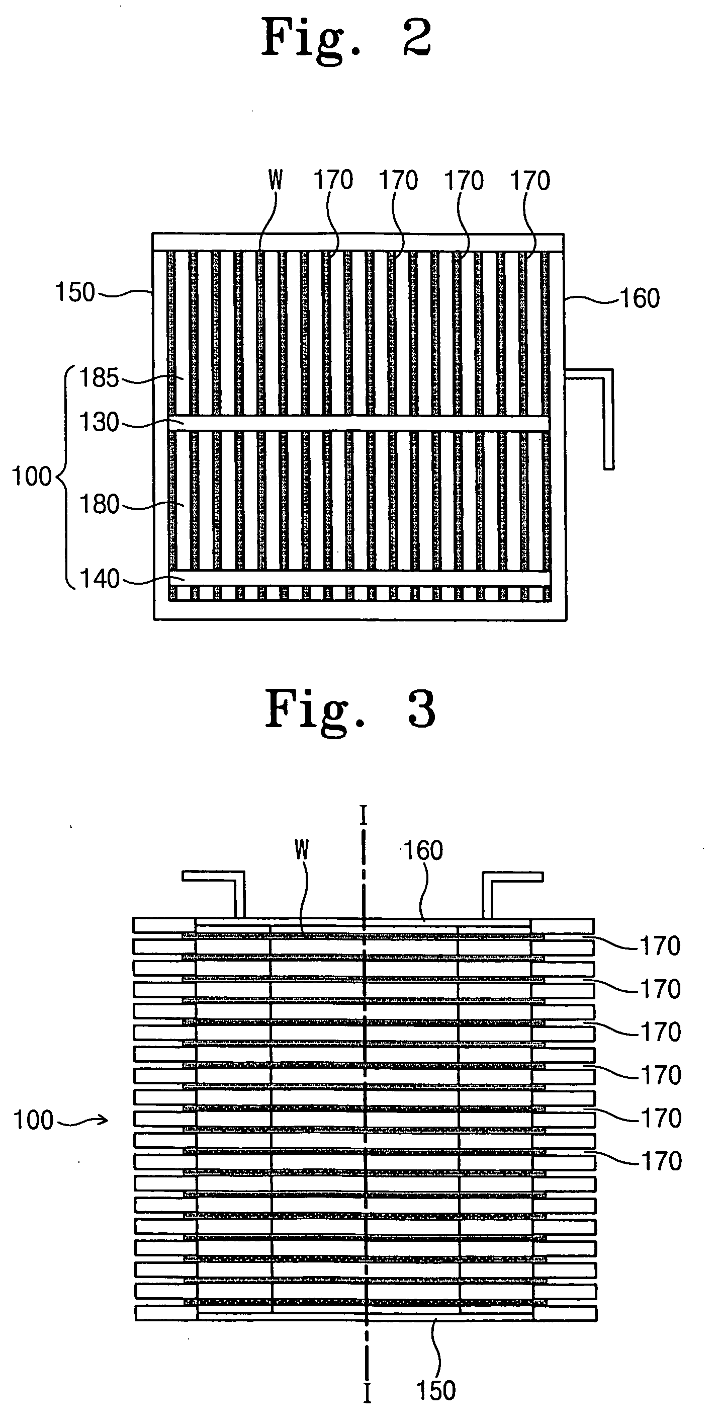
[0031]FIG. 2 is a side view of a wafer carrier according to an exemplary embodiment of the present invention, FIG. 3 is a plan view of the wafer carrier in FIG. 2, and FIG. 4 is a front view of the wafer carrier in FIG. 2.
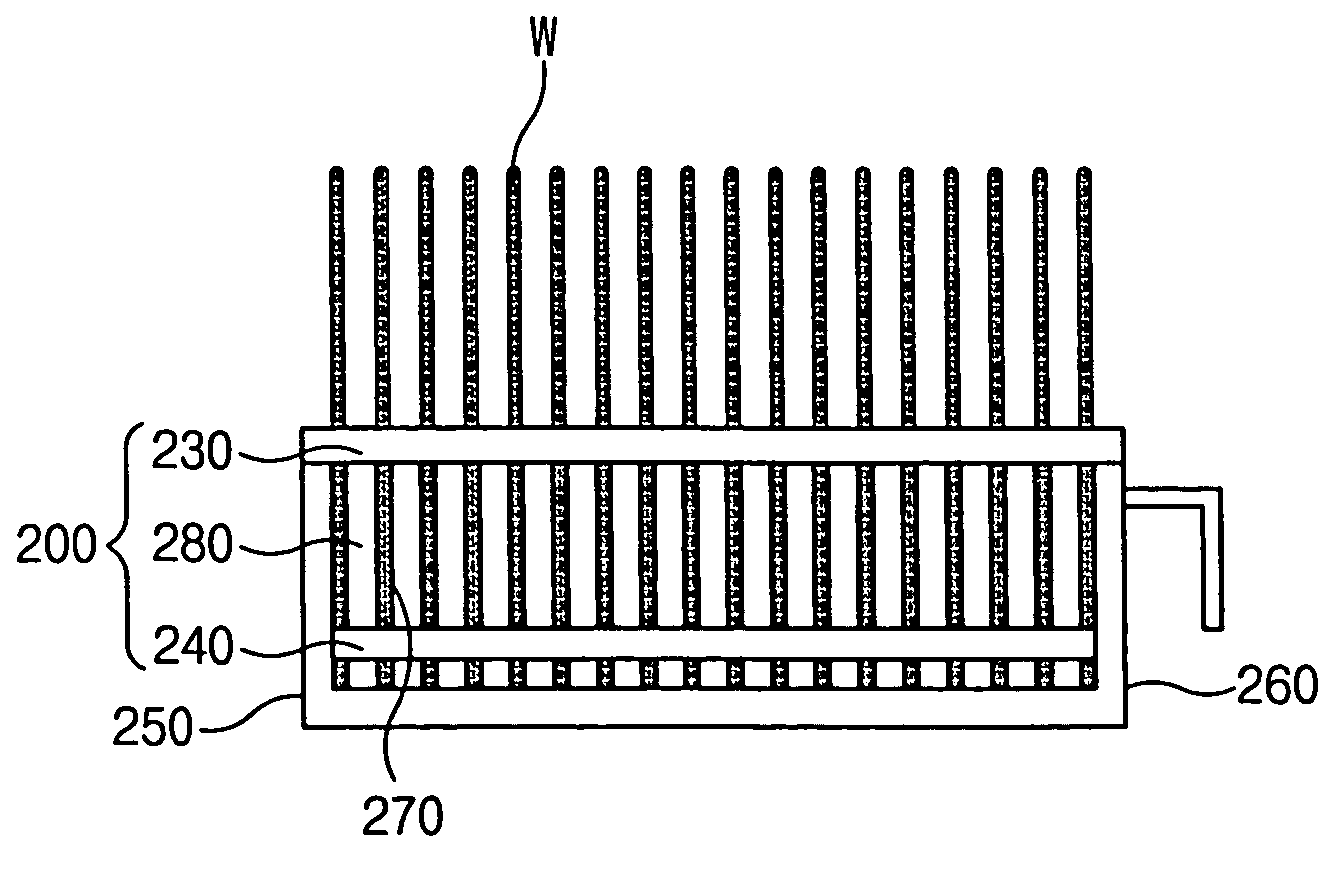
[0032] Referring to FIGS. 2 through 4, a wafer carrier according to an exemplary embodiment of the present invention includes a storage holding member 100 capable of storing a plurality of semiconductor wafers W upright and in a row with an adequate gap between the wafers. The wafer carrier also has a front fixing plate 150 and a rear fixing plate 160 disposed respectively at the front and rear of the wafer carrier along the axial line I of the storage holding member 100. The top and bottom of the wafer carrier are open.
[0033] The storage holding member 100 further includes a side support 130 disposed o...
PUM
 Abstract
Description
Claims
Application Information