Method of fabricating a semiconductor device

a semiconductor and semiconductor layer technology, applied in semiconductor/solid-state device manufacturing, basic electric elements, electric devices, etc., can solve the problems of easy deformation of si—chsub>3/sub>bonds, easy deformation of sog layers, and increased hygroscopicity of sog layers

Active Publication Date: 2006-09-28
RENESAS ELECTRONICS CORP
View PDF5 Cites 24 Cited by
  • Summary
  • Abstract
  • Description
  • Claims
  • Application Information

AI Technical Summary

Benefits of technology

[0013] This makes it possible to form an intermediate film composed of a SiO2 film. Formation of the intermediate film using this sort of material is successful in enhancing ashing resistance of the intermediate film. This makes it possible to prevent the intermediate film from degrading, even when the resist film was found to be misaligned after it was patterned, and so that the resist film had to be removed by ashing.
[0024] According to the present invention, it is made possible to raise etching resistance of the intermediate film, when interconnect trenches and viaholes of a semiconductor device are formed using the three-layered resist process.

Problems solved by technology

The removal of the upper resist film using an organic solvent has, however, also resulted in peeling off of SOG composing the intermediate film.
The conventional peeling off and removal of the upper resist film by O2 ashing has been known to promote bonding of C and O in SOG during the ashing, and to readily destruct Si—CH3 bonds.
Portions where the Si—CH3 bonds were destructed generate dangling bonds of Si, and this undesirably increases hygroscopicity of the SOG layer.
Such moisture absorption of the underlying SOG modifies film properties thereof, and this consequently alters light exposure conditions for the upper resist film, and results in pattern failure.
For this reason, it has been believed as being difficult to peel off and remove only the upper resist film and to re-build it in the three-layered resist technique using SOG, and as being poor in the mass productivity.

Method used


Image

  • Method of fabricating a semiconductor device
  • Method of fabricating a semiconductor device
  • Method of fabricating a semiconductor device

Examples


first embodiment

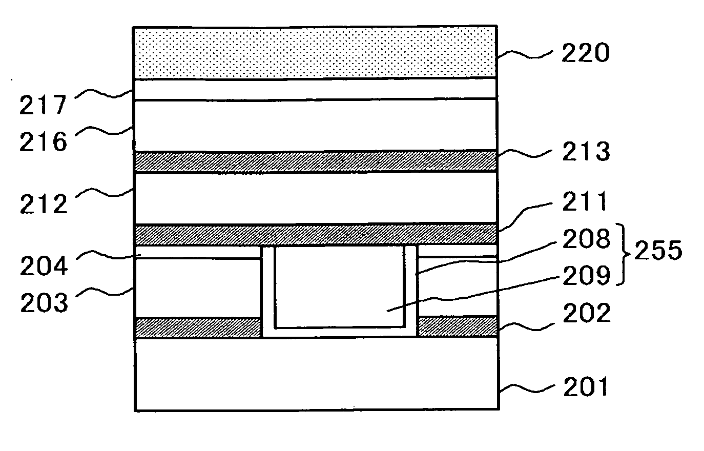
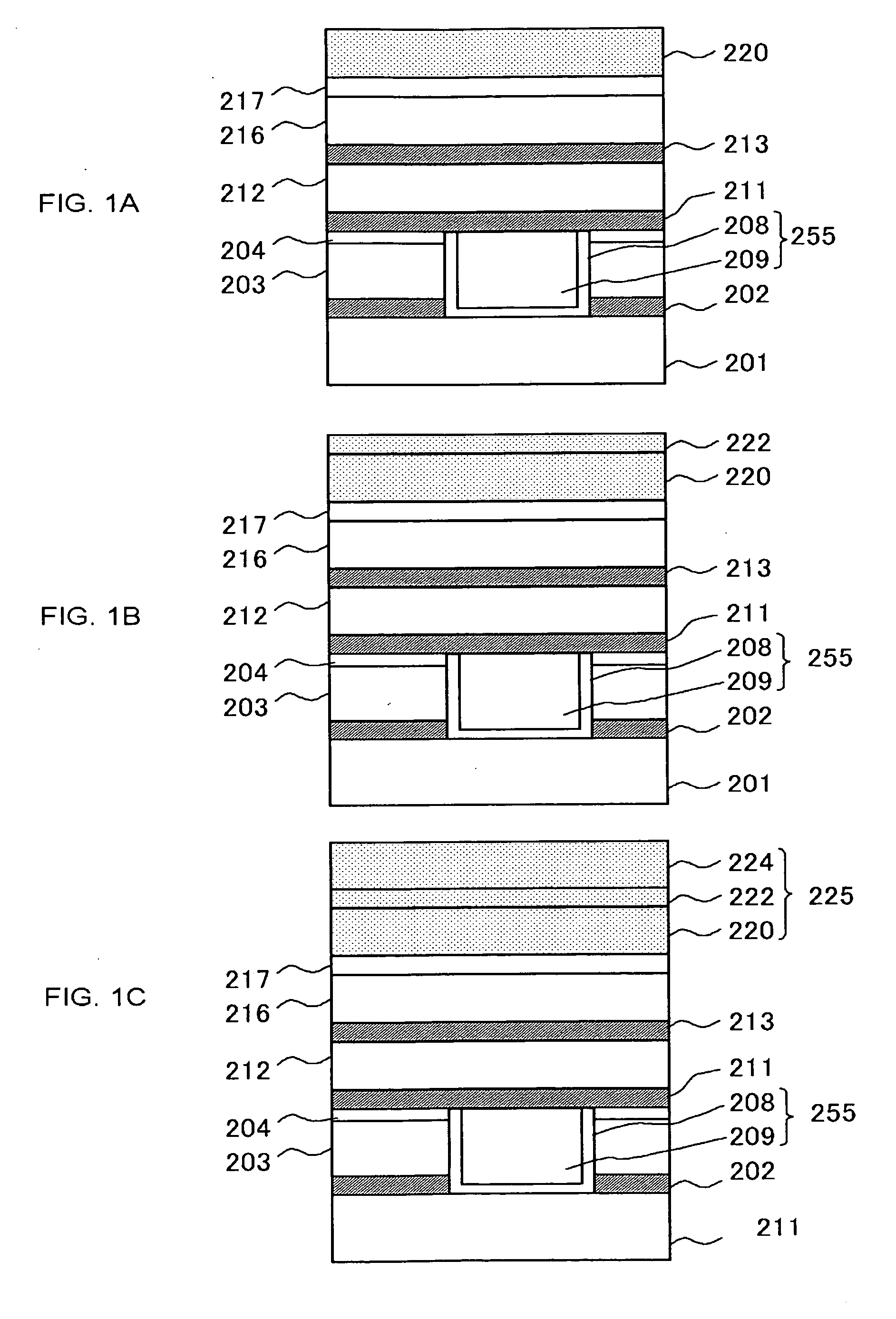
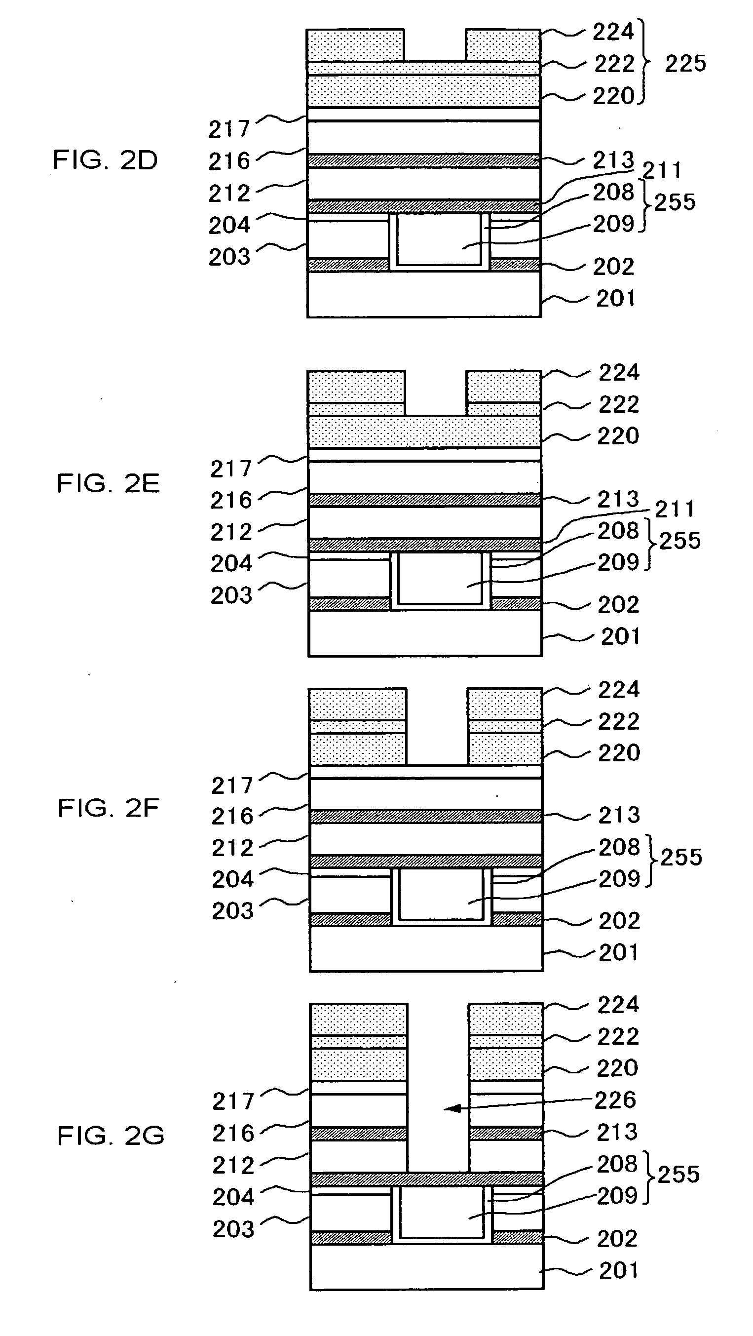
[0037]FIGS. 1A to 4L are step-wise sectional views showing procedures for fabricating a semiconductor device 200 according to the embodiment of the present invention.

[0038] This embodiment will describe an exemplary case where the present invention is applied to formation of a multi-layered wiring structure based on the dual-damascene process. The description herein will be made on a method of forming interconnects / wirings and vias by so-called, via-first process.

[0039] Procedures up to formation of a multi-layered wiring structure shown in FIG. 1A will be described. First, on an underlying insulating film 201 formed on a semiconductor substrate (not shown), an etching stopper film 202, a first interlayer dielectric film 203, and a first protective film 204 are sequentially stacked. The etching stopper film 202 is typically composed of a SiC film or a SiCN film.

[0040] The first interlayer dielectric film 203 can be configured using low-dielectric-constant materials such as polyhy...

second embodiment

[0062]FIG. 5 and FIG. 6 are structural drawings respectively showing the semiconductor device 200 according to the embodiment of the present invention. Detailed structure of the lower layers under the three-layered resist film 235 herein is not shown, simply referring to as an object-to-be-etched 229.

[0063] As shown in FIG. 5, the three-layered resist film 235 may also be configured as having an anti-reflection film 244 between the third resist film 230 and the intermediate film 232. The anti-reflection film 244 herein may be configured typically using SiON or SiOC. For an exemplary case where the anti-reflection film 244 is configured using SiON, SiON can be formed using SiH4 and N2O gases at 200° C. or below in a parallel-plate-type plasma CVD apparatus. The anti-reflection film 244 is preferably formed in the same apparatus in which the intermediate film 232 is formed. Enrichment of the Si composition of the anti-reflection film 244 can increase the attenuation coefficient of li...

example 1

[0067] Structural changes in a TEOS-SiO2 film, a SiH4—SiO2 film, and a SOG film before and after ashing were investigated. The individual films were prepared as follows.

i) TEOS-SiO2 Film

[0068] A mixed gas of TEOS and O2 (ratio of flow rate of 1:10) was used as a film forming gas, and the film was formed by the two-frequency plasma CVD process at 200° C. under a reduced pressure of approximately 3 Torr. Output power was adjusted to approximately 100 W for the higher frequency (13.56 MHz), and at approximately 200 W for the lower frequency (approximately 500 kHz).

ii) SiH4—SiO2 Film

[0069] The film was formed by the CVD process at 200° C., using a mixed gas of SiH4 and N2O (ratio of flow rate of 1:20), under a reduced pressure of approximately 3 Torr.

iii) SOG Film

[0070] A chemical liquid of SOG was dropped through a coater, sintered at approximately 200° C. on a hot plate, to thereby form the film.

[0071] Three thus-prepared films were subjected to O2 ashing at approximately 25...


PUM


Abstract

An intermediate film 222 in a three-layered resist film 225 is formed by the chemical vapor deposition process at a temperature not higher than 300° C., using Si(OR1)(OR2)(OR3)(OR4) , where each of R1, R2, R3 and R4 independently represents a carbon-containing group or a hydrogen atom, excluding the case where all of R1 to R4 are hydrogen atoms.

Description

[0001] This application is based on Japanese patent applications No. 2005-089794 and No. 2004-090575 the content of which are incorporated hereinto by reference. DISCLOSURE OF THE INVENTION [0002] 1. Field of the Invention [0003] The present invention relates to a method of fabricating a semiconductor device, by which interconnect trenches and viaholes are formed using the three-layered resist process. [0004] 2. Related Art [0005] With advancement in micronization of semiconductor devices, there are increasing demands on micro-fabrication in etching technology using photoresist. The three-layered resist process is known as a method allowing micro-fabrication unsusceptible to step difference on substrates. In the three-layered resist process, first, a thick lower resist film is coated on a substrate to be micro-fabricated. Next, SOG (spin-on-glass) is coated on the lower resist film to thereby form an intermediate film. Further thereon, an upper resist film is coated, the upper resis...

Claims


Application Information

Patent Timeline
Patent Type & Authority Applications(United States)
IPC IPC(8): H01L21/473
CPCH01L21/02164H01L21/02271H01L21/02274H01L21/31144H01L21/31612
Inventor USAMI, TATSUYAOHNISHI, SADAYUKIHIROI, MASAYUKIMATSUMOTO, AKIRA
Owner RENESAS ELECTRONICS CORP
Why Eureka
Try Eureka