Detecting apparatus and device manufacturing method

a technology of detection apparatus and manufacturing method, which is applied in the direction of heat measurement, semiconductor/solid-state device testing/measurement, instruments, etc., can solve the problems of reducing the accuracy of position and resolution, and reducing the cost

Inactive Publication Date: 2006-10-05
TOSHIBA MEMORY CORP
View PDF13 Cites 2 Cited by
  • Summary
  • Abstract
  • Description
  • Claims
  • Application Information

AI Technical Summary

Benefits of technology

[0011] For the flange structure and the feed through, the afore-mentioned one can be used. In order to improve signal transmission performance, a sensor package which integrates a sensor and signal transmission pins can be used. The sensor package has a function of a table for securing and wiring of the sensor. Wirings may be formed between a pad electrode on the surface of the sensor and a pad of the package by using bonder or the like. By using a sensor package with function of feed through, the wiring distance is reduced, and it is possible to improve transmission signal frequency property (e.g. by 20-30%) and to decrease noise (e.g. by 20-30%) of signals.
[0014] A detecting apparatus of the present invention comprises within a vacuum chamber, a mechanism for irradiating the secondary electrons or a reflected light emitted from the wafer, against the sensor, thereby eliminating the need for the optical lens, the FOP, the hermetic glass plate or fittings for them, so that advantageously, the number of components included in the detecting apparatus can be reduced, the accuracy of position and resolution can be improved, the possible deterioration of optical properties in transmission to the sensor can be dissolved, and the apparatus can be manufactured at a lower cost.

Problems solved by technology

However, the prior art detecting apparatus shown in FIG. 1 and FIG. 2 has such a drawback that the intensity of the light reaching the sensor has been attenuated since in this apparatus the light beam passes through the hermetic glass plate defining the inside and outside of the vacuum vessel and also through the lens and then enters the sensor in the atmosphere so as to be converted into the image signals for the sample surface.
The attenuation factor of this configuration is observed to be, for example, in the range of 1 / 20 to ½. In addition to the problem of the attenuation occurring in the intensity of the light, the prior art detecting apparatus also has another problem that the hermetic glass plate and / or the lens may cause an aberration or distortion in the light beam, inhibiting the capturing of highly accurate image.
Furthermore, the prior art apparatus still has another problem that use of many optical components and supporting and / or fixing parts thereof in the apparatus might sometimes cause a mechanical offset among the sensor, the hermetic glass and the lens, which also inhibit the capturing of highly accurate image.
Further, the apparatus shown in FIG. 2 using the conventional electronic optical system, in which the image information represented by the electrons is converted into light and then thus converted light is in turn detected, is also problematic in that the efficiency and resolution may deteriorate as a result of this conversion.

Method used


Image

  • Detecting apparatus and device manufacturing method
  • Detecting apparatus and device manufacturing method
  • Detecting apparatus and device manufacturing method

Examples


Embodiment Construction

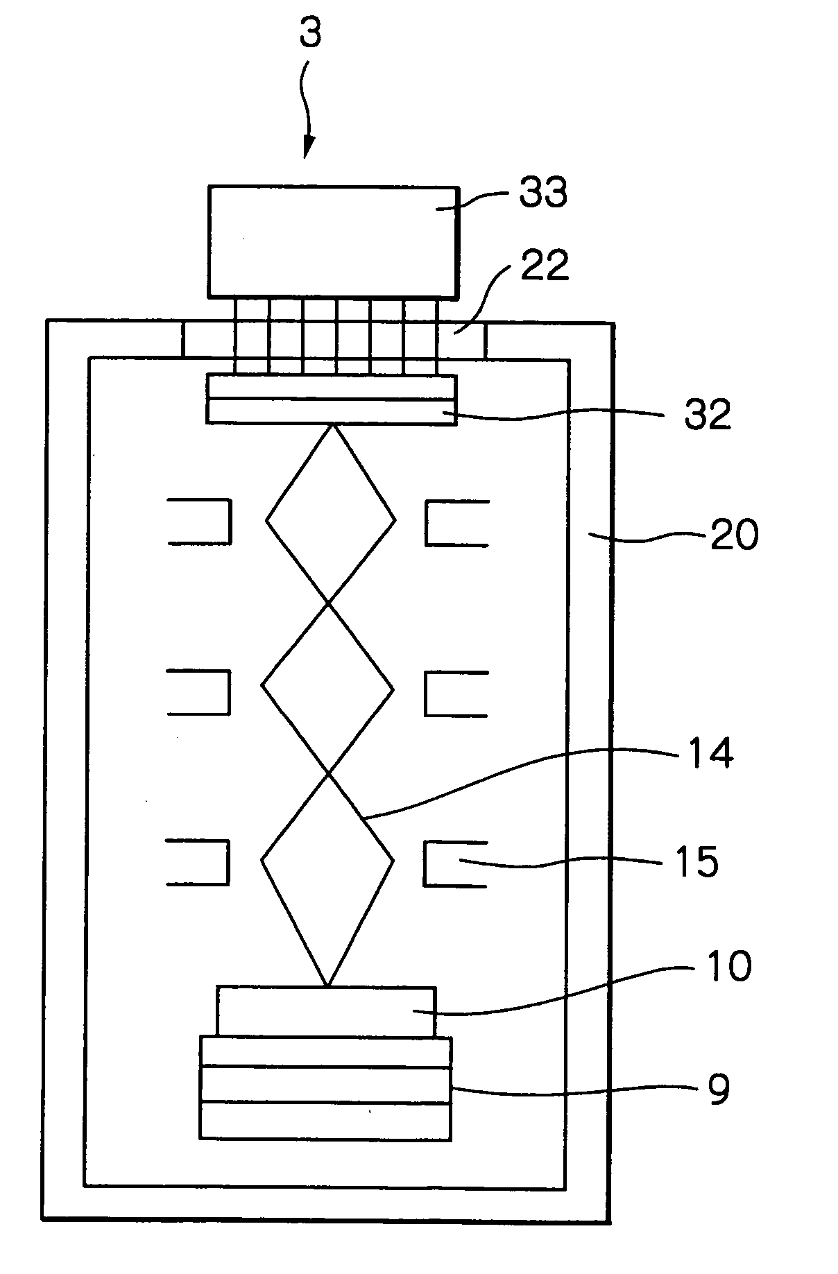
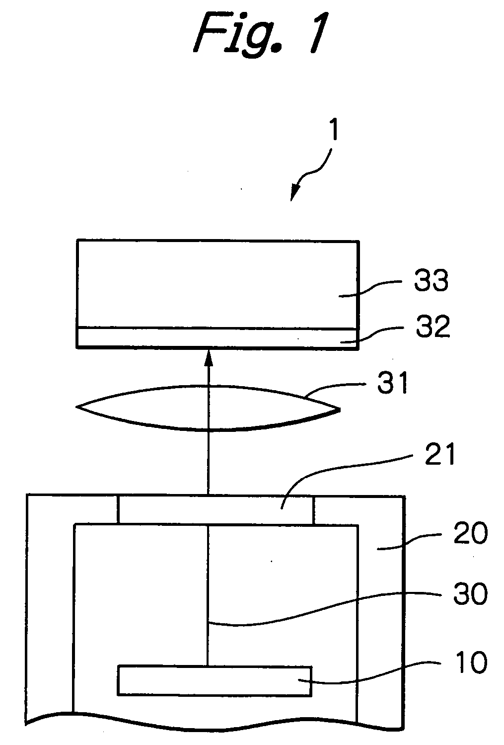
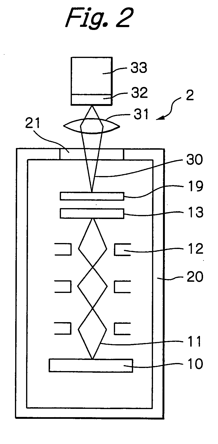
[0031]FIG. 3 through FIG. 8 show schematic diagrams of detecting apparatuses according to respective embodiments of the present invention, in which some elements corresponding to those of the detecting apparatuses shown in FIG. 1 and FIG. 2 are designated with the same reference numerals and the duplicated descriptions will be omitted. FIG. 3 is a schematic diagram of a detecting apparatus 3 containing a mapping optical system according to an embodiment of the present invention, in which a sensor 32 comprising an EB-CCD (Electron Beam detecting Charge Coupled Device) is disposed within a vacuum vessel 20. Components including a lens of an electronic optical system (an electrostatic lens) 15, an aperture, a stigmatic element (an element for generating an appropriate distribution of an electric field to compensate for astigmatism or spherical aberration) are disposed within the vacuum vessel 20. A sample 10 is a silicon wafer having a diameter of 300 mm and fixedly mounted on a stage ...


PUM

PropertyMeasurementUnit
wave lengthaaaaaaaaaa
diameteraaaaaaaaaa
diameteraaaaaaaaaa

Abstract

A detecting apparatus for detecting a fine geometry on a surface of a sample, wherein an irradiation beam is irradiated against the sample placed in a different environment different from an atmosphere and a secondary radiation emanated from the sample is detected by a sensor, and wherein the sensor is disposed at an inside of the different environment, a processing device to process detection signals from the sensor is disposed at an outside of the different environment, and a transmission means transmits detection signals from the sensor to the processing device.

Description

RELATED APPLICATION [0001] This application is a divisional of U.S. patent application Ser. No. 10 / 237,986 filed on Sep. 10, 2002, which is incorporated by reference in its entirety. Priority under 35 U.S.C. 120 and 121 is hereby claimed for benefit of the filing date of U.S. patent application Ser. No. 10 / 237,986.BACKGROUND OF THE INVENTION [0002] The present invention relates to a detecting apparatus for detecting a fine geometry (an image) on a surface of a sample by irradiating an irradiation beam against the sample and then detecting and processing a secondary radiation emanated from the sample. The fine geometry on the surface of the sample, for the purpose of the present invention, includes a defect in such a high density pattern having a minimum line width of 0.15 μm or smaller formed on a wafer surface of a semiconductor device, for example. The present invention also relates to a manufacturing method of a semiconductor device employing such a detecting apparatus. [0003] Th...

Claims


Application Information

Patent Timeline
Patent Type & Authority Applications(United States)
IPC IPC(8): G21K7/00G01N23/00H01L21/66G01B15/00G01N21/95G03F1/00G03F1/84H01J37/16H01J37/244H01J37/29
CPCG01N21/9501G03F1/0092H01J2237/2446H01J37/285H01J2237/2441H01J37/244G03F1/84H01L22/00
Inventor HATAKEYAMA, MASAHIROMURAKAMI, TAKESHISATAKE, TOHRUNOJI, NOBUHARUNAGAHAMA, ICHIROTAYAMAZAKI, YUICHIRO
Owner TOSHIBA MEMORY CORP
Why Eureka
Try Eureka