
Scanning electron microscope

a scanning electron microscope and microscope technology, applied in the field can solve the problems of inability to improve the installation environment of scanning electron microscopes, inability to detect vibrations from the floor surface, and inability to achieve high-resolution scanning electron microscopes, so as to achieve easy and fast correction of the pixel position

Inactive Publication Date: 2006-10-05
JEOL LTD
View PDF2 Cites 6 Cited by
  • Summary
  • Abstract
  • Description
  • Claims
  • Application Information

AI Technical Summary

Benefits of technology

[0012] It is an object of the present invention to provide a scanning electron microscope which can detect variations in the relative position between a container having a specimen therein and a specimen stage located within the container and carrying the specimen thereon and which can remove the effects of vibrations on image information easily and reliably.
[0036] According to the eighth embodiment of the present invention, the image creation means creates new image information by calculating interpolated values of each dropout pixel position from image information at plural pixel positions adjacent to the dropout pixel position or from plural images obtained at successive instants of time at the same pixel position. Therefore, any pixel position at which no image information is present can be eliminated. Appropriate image information can be obtained.

Problems solved by technology

In the former environments, vibrations from the floor surface inevitably enter the instrument.
This is undesirable for high-magnification, high-resolution scanning electron microscopes.
Furthermore, strengthening of the floor surface and improvement of the installation environments of scanning electron microscopes may involve difficulties because of costs or because the purpose is to inspect finished products incorporated in a production process.
However, the effects of variations in the relative position between the specimen stage and the specimen chamber on the image information are not easily removed with any one of the prior art techniques described above.
Even if the rigidity of the portion located between the specimen stage and the specimen chamber is improved, it is difficult to remove vibrations comparable to such a resolution.
Furthermore, when vibrations of the portion located between the specimen stage and the specimen chamber are detected and the beam hit position is controlled using the resulting detection signal, error is produced due to delay of the control.

Method used


Image

  • Scanning electron microscope
  • Scanning electron microscope
  • Scanning electron microscope

Examples


Embodiment Construction

[0043] The preferred embodiments of a scanning electron microscope according to the present invention are hereinafter described with reference to the accompanying drawings. It is to be noted that the invention is not limited thereto.

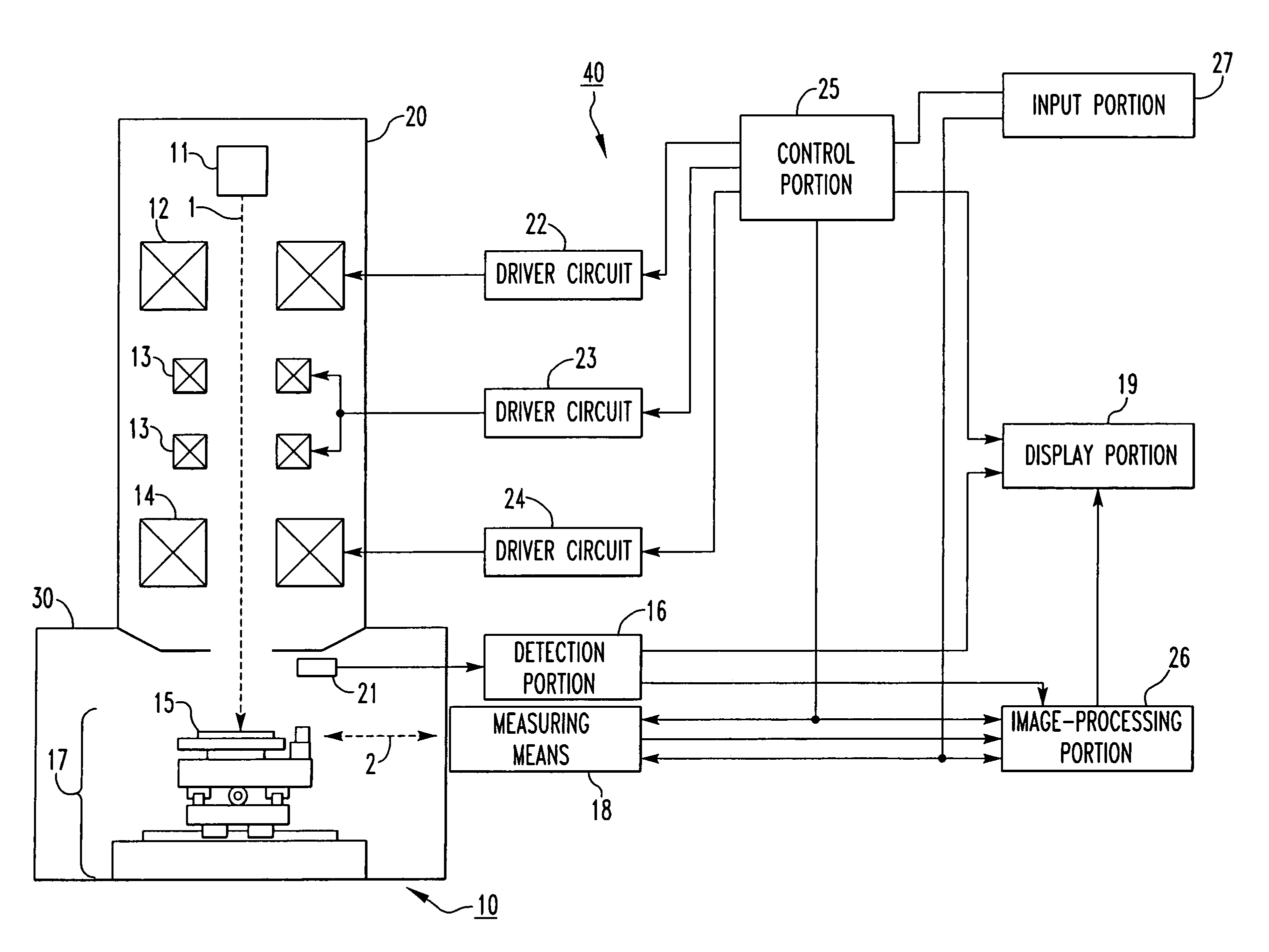
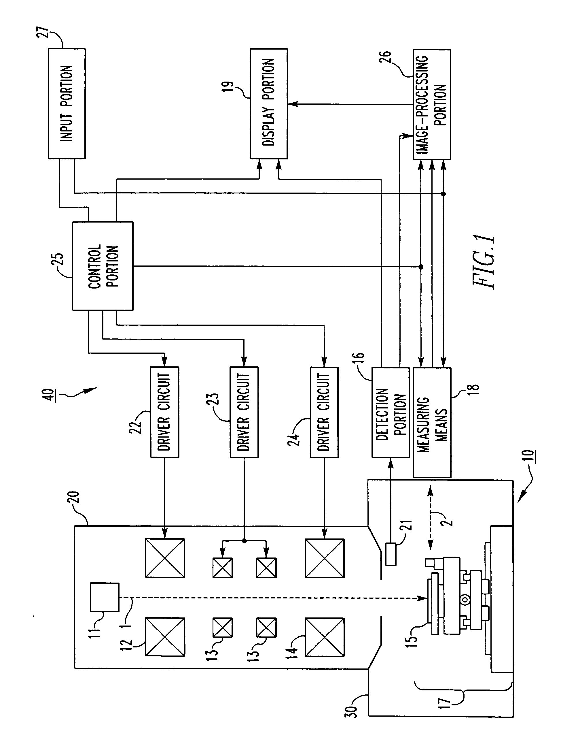
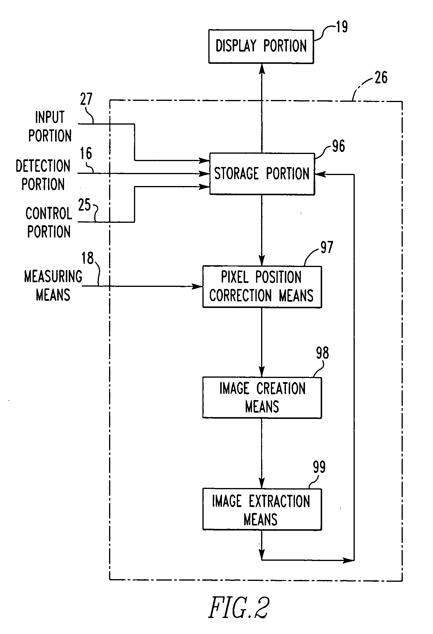
[0044] A scanning electron microscope according to an embodiment of the present invention is generally indicated by reference numeral 10 in FIG. 1, which is a cross-sectional view showing the whole structure of the microscope 10. The microscope 10 consists of a microscope column portion 20, a specimen chamber 30, and circuitry 40. The microscope column portion 20 includes an electron gun 11, condenser lenses 12, deflection coils 13, and an objective lens 14. The specimen chamber 30 includes a specimen stage section 17. A specimen 15 is placed inside the chamber 30. The circuitry 40 includes driver circuits 22-24, a control portion 25, a detection portion 16 including sensors 21, an input portion 27, a display portion 19, a measuring means 18, and an ima...


PUM

PropertyMeasurementUnit
scanning electron microscopeaaaaaaaaaa
capacitance displacement gaugeaaaaaaaaaa
timeaaaaaaaaaa

Abstract

There is disclosed a scanning electron microscope capable of removing the effects of vibrations on image information easily and reliably by detecting variations in the relative position between a specimen chamber holding a specimen therein and the specimen stage. The microscope has an image-processing portion that obtains information about the relative position between the specimen stage and the specimen chamber from a measurement unit when the beam is scanned. Based on the information about the relative position, a pixel position-correcting unit makes corrections to pixel positions indicated by the image information obtained by the scanning. An image creation unit creates image elements to eliminate pixel dropouts or pixel duplication produced by the aforementioned corrections. An image extraction unit extracts an image to be displayed.

Description

BACKGROUND OF THE INVENTION [0001] 1. Field of the Invention [0002] The present invention relates to a scanning electron microscope for scanning a specimen placed on a specimen stage by an electron beam and obtaining image information about the specimen based on the scanning. [0003] 2. Description of Related Art [0004] In recent years, scanning electron microscopes have been used not only in scientific purposes but also for product inspections during various process steps in a manufacturing plant or at the time of shipment. For example, in semiconductor fabrication plants, scanning electron microscopes are used to inspect photolithographically defined silicon wafers. Inspections making use of high magnifications and high resolutions of scanning electron microscopes have become increasingly indispensable. [0005] On the other hand, environments where a scanning electron microscope within a manufacturing plant is installed are different from environments where a scanning electron micro...

Claims


Application Information

Patent Timeline
Patent Type & Authority Applications(United States)
IPC IPC(8): G21K7/00G01N23/00
CPCG01N23/225H01J37/153H01J2237/221H01J2237/0216H01J2237/20292H01J37/28
Inventor MIYAO, HIROFUMI
Owner JEOL LTD
Features
  • Generate Ideas
  • Intellectual Property
  • Life Sciences
  • Materials
  • Tech Scout
  • Unparalleled Data Quality
  • Higher Quality Content
  • 60% Fewer Hallucinations
Learn More