Semiconductor device and manufacturing method of the same

a technology of semiconductor devices and manufacturing methods, applied in semiconductor devices, basic electric elements, electrical appliances, etc., can solve the problems of inability to meet inability to achieve satisfactory electric properties of high-dielectric constant transistors, and inability to achieve high-speed operation at a low threshold voltage. , to achieve the effect of reducing gate leakage current, satisfying transistor electric properties, and improving device integration

Inactive Publication Date: 2006-10-05
FUJITSU SEMICON LTD
View PDF7 Cites 3 Cited by
  • Summary
  • Abstract
  • Description
  • Claims
  • Application Information

AI Technical Summary

Benefits of technology

[0013] The present invention is made in view of the aforementioned problem and its object is to provide a semiconductor device capable of obtaining satisfactory electric properties of transistors (for example, reduction in gate leakage current, operating life extension, and so on) by recovering surface damage due to etching and higher integration of the device by increasing design flexibility when a first gate insulating film and a second gate insulating film are separately formed on a first active region and a second active region, respectively, and a manufacturing method of the same.

Problems solved by technology

However, this high dielectric constant transistor is not suitable for high-speed operation at a low threshold voltage since the threshold voltage shifts to the high-voltage side.
However, in the case of Patent Documents 1 and 2, when the second gate insulating film is patterned, surface damage due to etching is inevitably caused to the first gate insulating film when the second gate insulating film on the first gate insulating film is removed by etching.
If the transistors are formed in this state, satisfactory electric properties of the transistors (for example, reduction in gate leakage current, operating life extension, and so on) cannot be obtained.

Method used


Image

  • Semiconductor device and manufacturing method of the same
  • Semiconductor device and manufacturing method of the same
  • Semiconductor device and manufacturing method of the same

Examples


modified example

[0078] Now, the modified example of the embodiment will be described.

[0079] In this modified example, similarly to the embodiment, a manufacturing method of a MIS transistor is disclosed, but is different in that preliminary surface recovery treatments are performed prior to the aforementioned surface recovery treatment.

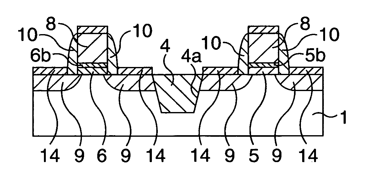
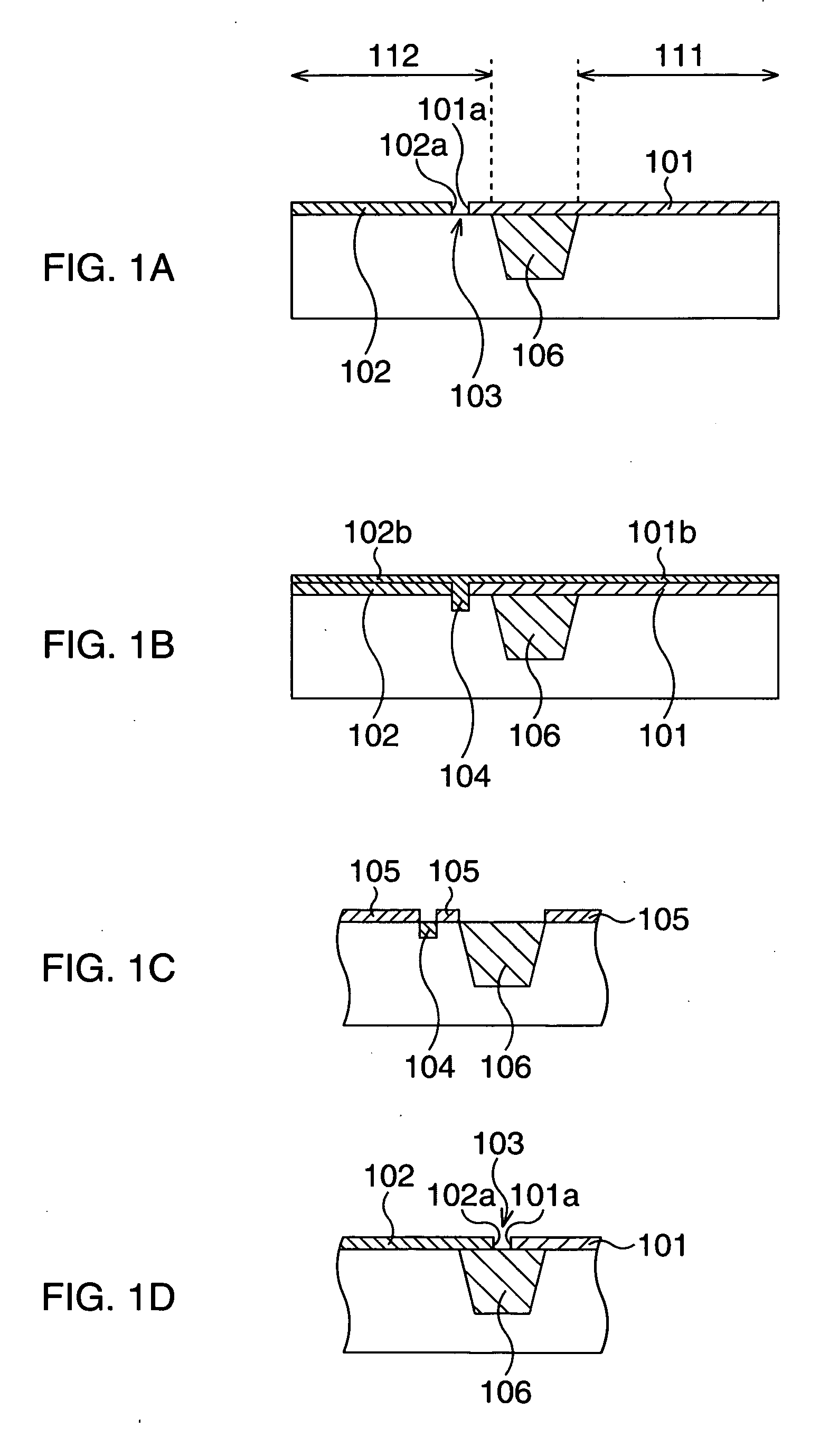
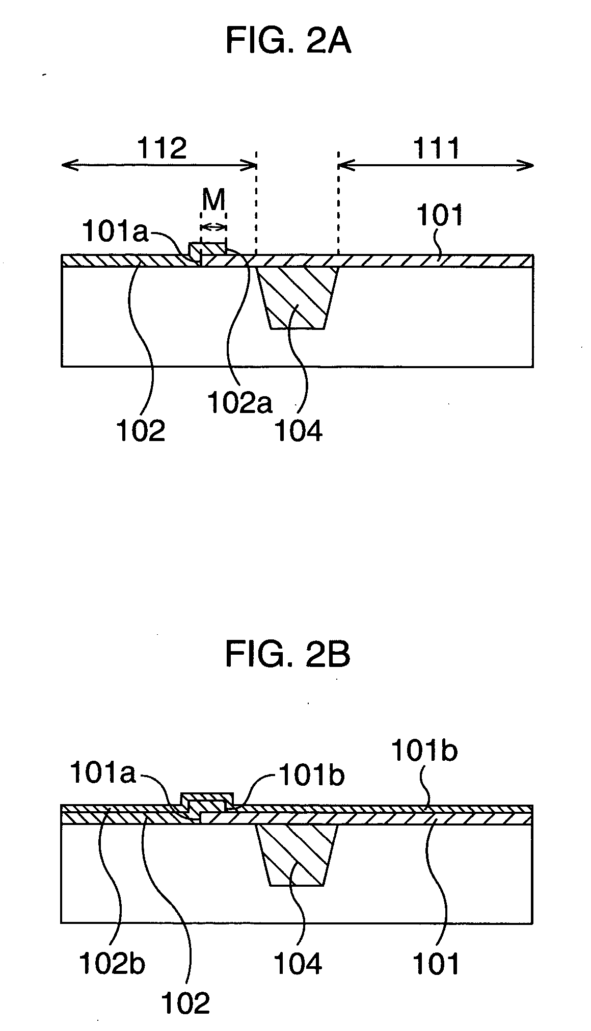
[0080]FIG. 7A to FIG. 7C are schematic sectional views showing only main steps of the manufacturing method of the MIS transistors according to this modified example. Incidentally, the same numerals and symbols will be used to designate the same components as those disclosed in the embodiment, so that a detailed description thereof will be omitted.

[0081] In this modified example, prior to the surface recovery treatment shown in FIG. 4C, the preliminary surface recovery treatment is individually performed on each of the first and second gate insulating films 5 and 6. Here, as the preliminary surface treatment described later, the nitriding treatment or the oxynitrid...


PUM


Abstract

Patterning is performed in such a manner that an end portion fabricated of a second gate insulating film partially overlaps an end portion fabricated of a first gate insulating film. Then, a surface recovery treatment is performed in the aforementioned state where the first and second gate insulating films partially overlap each other.

Description

CROSS-REFERENCE TO RELATED APPLICATIONS [0001] This application is based upon and claims the benefit of priority from the prior Japanese Patent Application No. 2005-096089, filed on Mar. 29, 2005, the entire contents of which are incorporated herein by reference. BACKGROUND OF THE INVENTION [0002] 1. Field of the Invention [0003] The present invention relates to a semiconductor device including two types of MIS transistors and a manufacturing method of the same, and particularly is suitable for application to a semiconductor device using a high dielectric constant material for a gate insulating film of one of the MIS transistors. [0004] 2. Description of the Related Art [0005] In recent years, as a transistor whose gate leakage current is small and power consumption is low, a MIS transistor using a gate insulating film made of a high dielectric constant material (hereinafter abbreviated only as a high dielectric constant transistor) attracts attention. However, this high dielectric ...

Claims


Application Information

Patent Timeline
Patent Type & Authority Applications(United States)
IPC IPC(8): H01L29/45
CPCH01L21/823481H01L21/823462
Inventor IKEDA, KAZUTO
Owner FUJITSU SEMICON LTD
Why Eureka
Try Eureka