Crack stop and moisture barrier

a moisture barrier and crack stop technology, applied in semiconductor devices, semiconductor/solid-state device details, electrical devices, etc., can solve problems such as device failure, disrupt conductive lines, damage to integrated circuits, etc., to reduce the area of chemical mechanical polishing (cmp) dishing around the chip edge. , the effect of easy implementation into semiconductor designs

Active Publication Date: 2006-10-05
INFINEON TECH AG
View PDF10 Cites 50 Cited by
  • Summary
  • Abstract
  • Description
  • Claims
  • Application Information

AI Technical Summary

Benefits of technology

[0011] Advantages of preferred embodiments of the present invention include providing a novel crack stop and moisture barrier that is easily implemented into semiconductor designs. Because the crack stop comprises a plurality of discrete features, etch processes to form the crack stop are readily implemented into manufacturing processes. Chemical mechanical polishing (CMP) dishing around the chip edge area is reduced. Integrated circuits with good quality and high reliability result from the use of the novel crack stop and moisture barrier designs described herein.

Problems solved by technology

A problem that can occur in integrated circuits is that when the die are singulated, the material layers can crack proximate the scribe line, damaging the integrated circuits and leading to device failures.
The cracks can disrupt conductive lines, for example, rendering the circuits inoperable.
The cracks can also allow moisture and other contaminants to enter into the integrated circuit, causing corrosion, for example.

Method used


Image

  • Crack stop and moisture barrier
  • Crack stop and moisture barrier
  • Crack stop and moisture barrier

Examples


Embodiment Construction

[0023] The making and using of the presently preferred embodiments are discussed in detail below. It should be appreciated, however, that the present invention provides many applicable inventive concepts that can be embodied in a wide variety of specific contexts. The specific embodiments discussed are merely illustrative of specific ways to make and use the invention, and do not limit the scope of the invention.

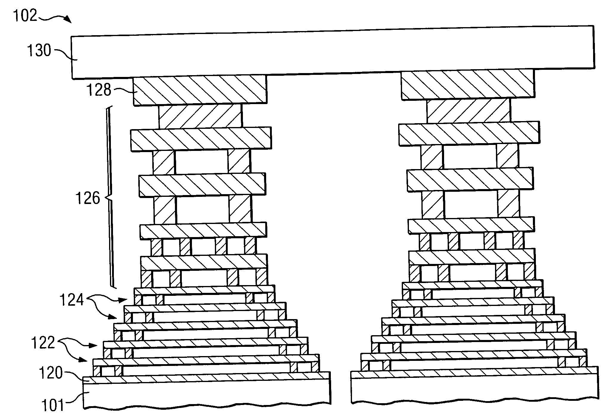
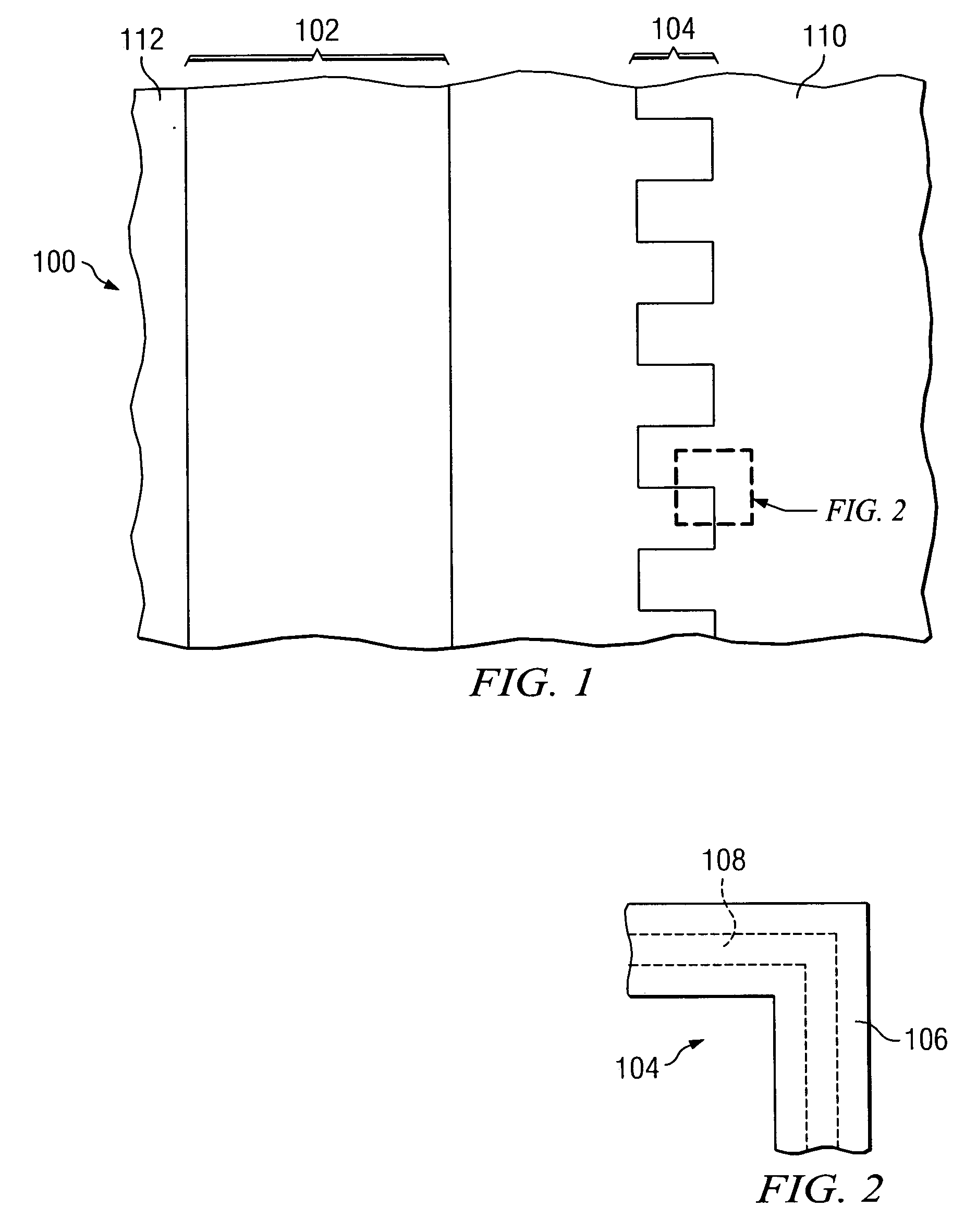
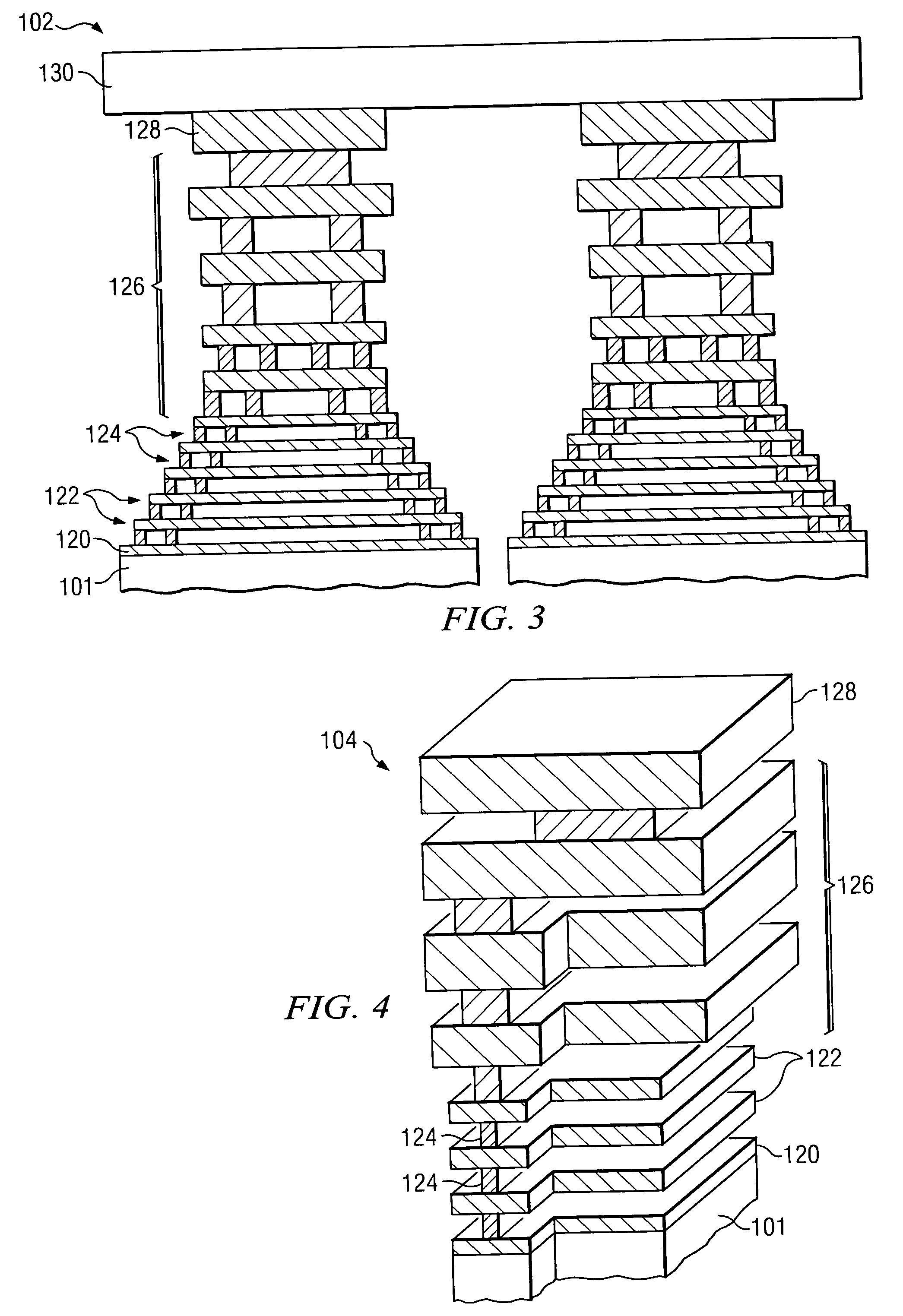
[0024] The present invention will be described with respect to preferred embodiments in a specific context, namely a crack prevention (also referred to herein as a crack stop) and moisture barrier structure for semiconductor devices. The invention may also be applied, however, to other applications where crack prevention structures are required, for example. The crack prevention structures described herein are preferably formed in metallization layers of an integrated circuit, although they may also be implemented in semiconductive material layers or insulating material lay...


PUM


Abstract

A design for a crack stop and moisture barrier for a semiconductor device includes a plurality of discrete conductive features formed at the edge of an integrated circuit proximate a scribe line. The discrete conductive features may comprise a plurality of staggered lines, a plurality of horseshoe-shaped lines, or a combination of both.

Description

TECHNICAL FIELD [0001] The present invention relates generally to the manufacture of semiconductor devices, and more particularly to a crack stop and moisture barrier design. BACKGROUND [0002] Semiconductor devices are used in a variety of electronic applications, such as personal computers, cell phones, digital cameras, and other electronic equipment, as examples. Semiconductor devices are typically fabricated by sequentially depositing insulating or dielectric layers, conductive layers, and semiconductive layers of material over a semiconductor substrate, and patterning the various layers using lithography to form circuit components and elements thereon. [0003] Dozens or hundreds of integrated circuits are typically manufactured on a single semiconductor wafer. The individual die are singulated by sawing the integrated circuits along a scribe line. The individual die are then packaged, either separately or in a multi-chip module or other type of packaging, for example. [0004] A pr...

Claims


Application Information

Patent Timeline
Patent Type & Authority Applications(United States)
IPC IPC(8): H01L23/52
CPCH01L23/562H01L23/564H01L23/585H01L2924/0002H01L2924/00
Inventor KIM, SUN-OOPARK, O SEO
Owner INFINEON TECH AG
Why Eureka
Try Eureka