

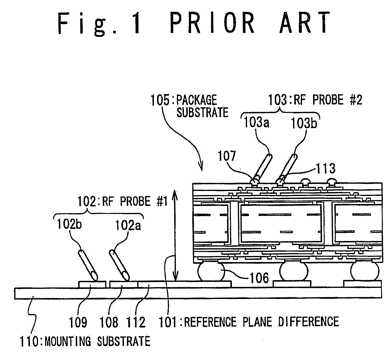
Impedance measuring apparatus of package substrate and method for the same
a technology of impedance measurement and substrate, which is applied in the direction of resistance/reactance/impedence, measurement devices, instruments, etc., can solve the problems of loss and measurement error, phase difference, and large measurement error in a lower frequency range, and achieve the effect of sufficient accuracy
- Summary
- Abstract
- Description
- Claims
- Application Information
AI Technical Summary
Benefits of technology
Problems solved by technology
Method used
Image

Examples
first embodiment
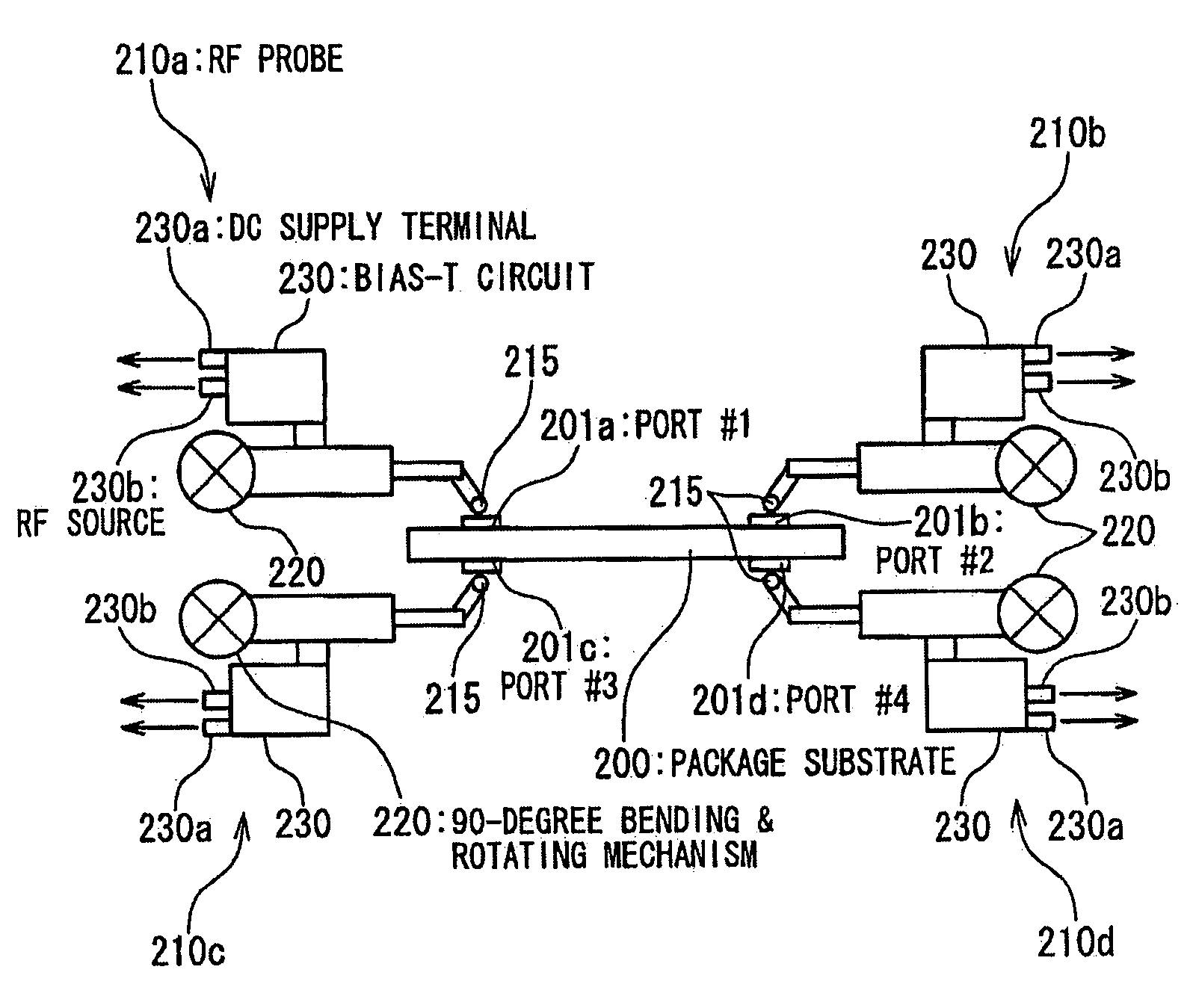
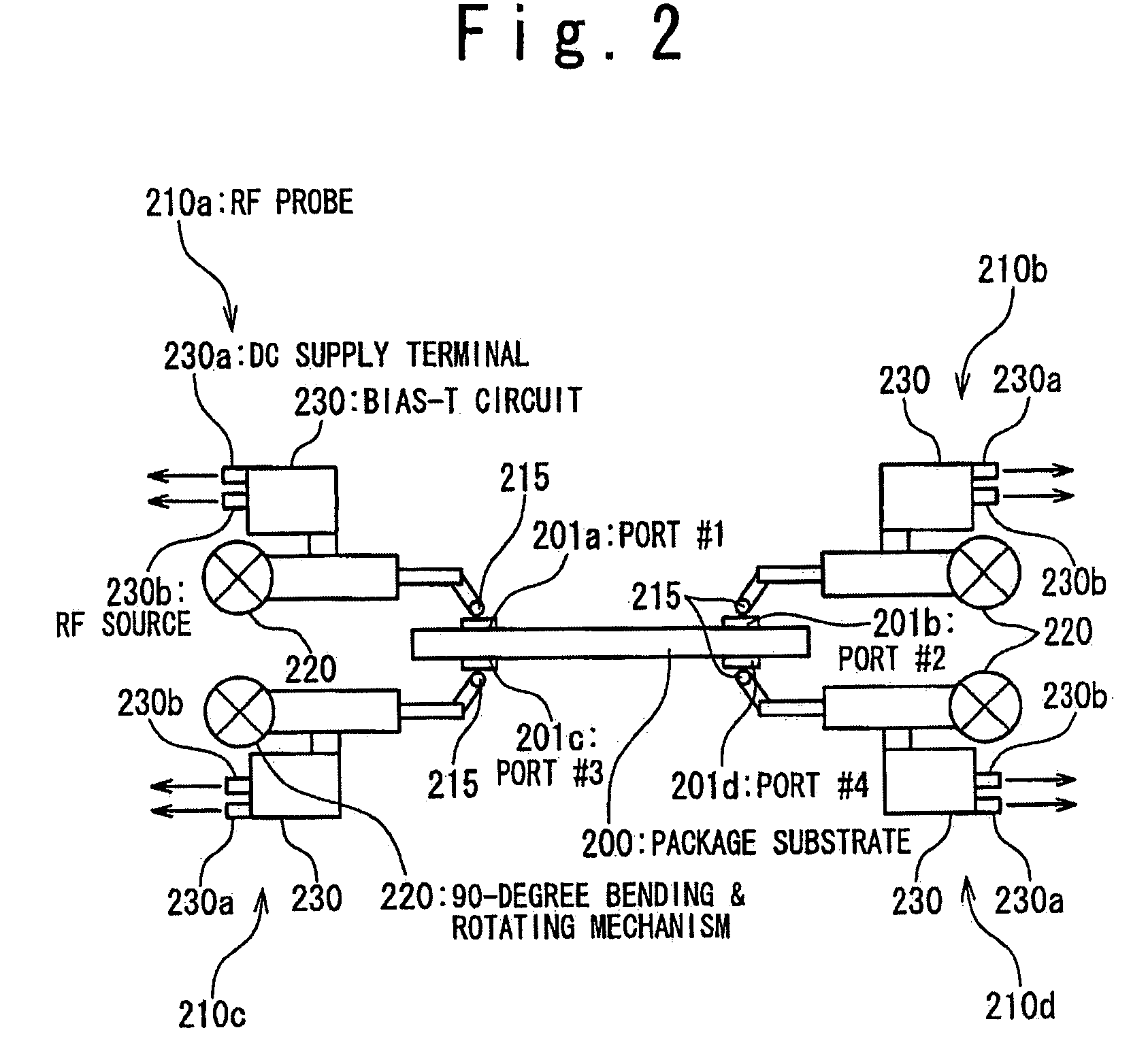
[0041]FIG. 2 is a cross sectional view schematically showing the structure of the impedance measuring apparatus according to the first embodiment of the present invention when a package substrate 200 as a measurement target is measured.
[0042] The impedance measuring apparatus in the first embodiment includes a processing unit (not shown) containing a network analyzer (not shown) and carrying out a calibration calculation, four RF (radio frequency) probes 210a to 210d, a 90-degree bending & rotating mechanism 220 connected to each of the RF probes 210a to 210d, a calibration substrate supporting mechanism 250 to support calibration substrates 240 (FIG. 3) in a horizontal or vertical state, and a mechanical controller (not shown). The mechanical controller (not shown) controls the rotation mechanisms 220 to be rotated.
[0043] Each of the RF probes 210a to 210d includes a DC supply terminal 230a, a Bias-T circuit 230 and a signal probe 215. The DC supply terminal 230a receives a DC vo...
second embodiment
[0052]FIGS. 5 and 6 are diagram schematically showing the impedance measuring apparatus of the package substrate according to the second embodiment of the present invention. The basic configuration and operation principle of the impedance measuring apparatus in the second embodiment are the same as those in the first embodiment. However, a 180-degree bending & rotating mechanism 420 is provided in the second embodiment instead of the 90-degree bending & rotating mechanism 250.
[0053] The RF impedance measuring apparatus in the second embodiment includes two RF probes 410a and 410b, and the above-mentioned 180-degree bending & rotating mechanisms 420. Each of the RF probes 410a and 410b includes a DC supply terminal 430a to receive a DC bias, and a Bias-T circuit 430 to receive and combine the DC bias from the DC supply terminal 430a and an RF signal from the processing unit (not shown), and a signal probe 415. The Bias-T circuit 430 supplies the combined RF signal to a substrate thr...
third embodiment
[0058]FIG. 7 is a diagram schematically showing the RF impedance measuring apparatus of a package substrate according to the third embodiment of the present invention. The basic structure and measurement principles in the third embodiment are the same as those the second embodiment. However, the third embodiment includes scales for accurately measuring the position coordinates of RF probes 410a and 410b with respect to the three axis directions as shown in FIG. 7. Thus, the thickness (in Z direction) of the package substrate 400 and the distance between ports in within the same plane (XY plane) of the package substrate 400 can be accurately measured, thereby the phase correction can be carried out promptly and easily.
[0059] The RF impedance measuring apparatus of the third embodiment includes two RF probes 410a and 410b, two RF probe supporting mechanisms 450a and 450b to support the two RF probes 410a and 410b, and the 180-degree bending & rotating mechanism 420. As shown in FIG. ...
PUM
 Abstract
Description
Claims
Application Information