Integrated electronic non volatile memory device having NAND structure

a non-volatile memory, integrated technology, applied in static storage, digital storage, instruments, etc., can solve the problems of serious difficulties in acceding to a sector, nand memory does not allow a fast random access to the same, and the nand access protocol is quite slow in random access, so as to achieve the effect of minimizing the cell network

Active Publication Date: 2006-10-12
MICRON TECH INC
View PDF5 Cites 11 Cited by
  • Summary
  • Abstract
  • Description
  • Claims
  • Application Information

AI Technical Summary

Benefits of technology

[0028] A further object of the present invention is that of providing a type of memory electronic device wherein the two portions of memory matrix having different data storage capacity and different access speed can exploit the same structural sources but can be decoupled according to the operation needs by the user.
[0029] Still a further object of the invention is that of providing the introduction, with respect to the traditional methods, of a selection of the matrix rows so as to minimize the cell network and make more simple the realization thereof.

Problems solved by technology

However, although having the feature of a superior data modify speed, such NAND memories do not allow a fast random access to the same, since they are oriented to readings of entire pages of at least 512 bytes, but not of the single bytes.
In fact, the NAND access protocol is quite slow in random access due to the known latency time, and it exhibits serious difficulties for acceding into a sector or a page in a random way.
Secondly, the costs of the resulting package cannot differ significantly from the global cost of the various components, since they cannot exploit large scale economies in the realization of devices assembled with components being different from one another.
There exist, then, a series of problems to be faced starting from the assumption that only a detailed comprehension of the phenomena apt to the memorization of the data inside the memory cells can allow understanding of the intrinsic limits of the adopted technology.
This field suffers from the length of the memory cell arrays which require high propagation times in the reading step for allowing reaching the cells being farthest from the node to which the reading potential is applied.
Moreover, it is also to be noted that the lithographic sizes for the manufacturing of non-volatile memories have reached limits lower than about 65 nm, or even than 32 nm, such as to make not only the construction of the interface between the decoding circuitry and the matrix of the cells themselves difficult, but also such as to enormously increase the propagation times of the signals due to the lines length.
This is particularly true where the row lines reach the extreme compactness levels, mainly in Flash of the NAND type, the problem becomes extreme and the implementation complex to such an extent as to make the area occupation inefficient.
Well, even due to this the reading step is slowed down a lot.
This implies that each stack elemental structure has a very reduced conductivity being thus a great limitation to the reading speed.
The conventional stack structure (16, 32 cells) is thus intimately slow since it is not very conductive.
The reason of such slowness is due to the particular organization of the matrix which normally comprises groups of 16 / 32 cells in series which strongly reduces its conductivity, connected to each other through long selector lines which significantly decreases their propagations with long bit-lines which strongly burden the load.

Method used


Image

  • Integrated electronic non volatile memory device having NAND structure
  • Integrated electronic non volatile memory device having NAND structure
  • Integrated electronic non volatile memory device having NAND structure

Examples


Embodiment Construction

[0060] With reference to the Figures, and in particular to the example of FIG. 2, a memory electronic device realized according to the present invention and monolithically integrated on semiconductor is globally and schematically indicated at 20.

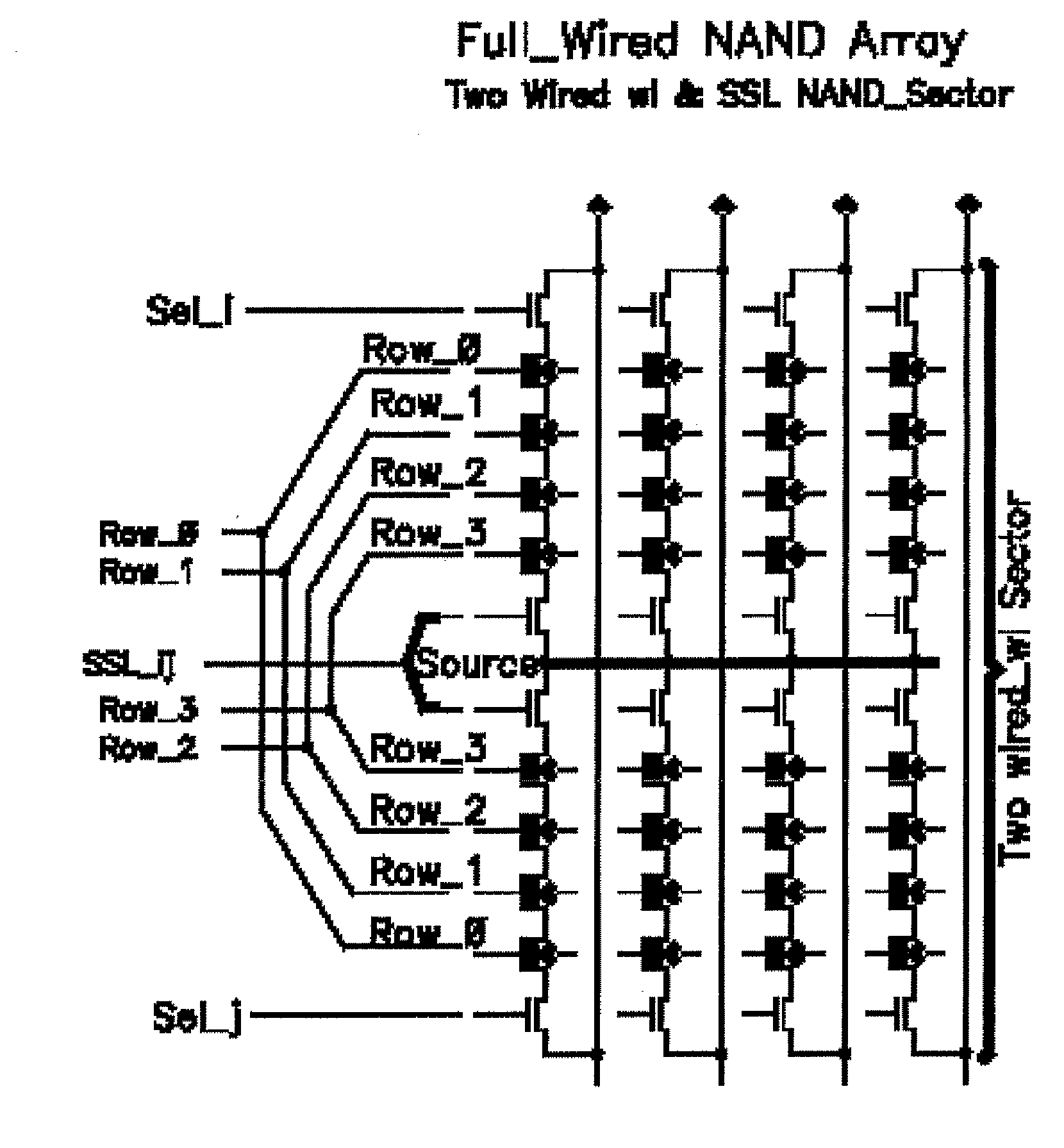
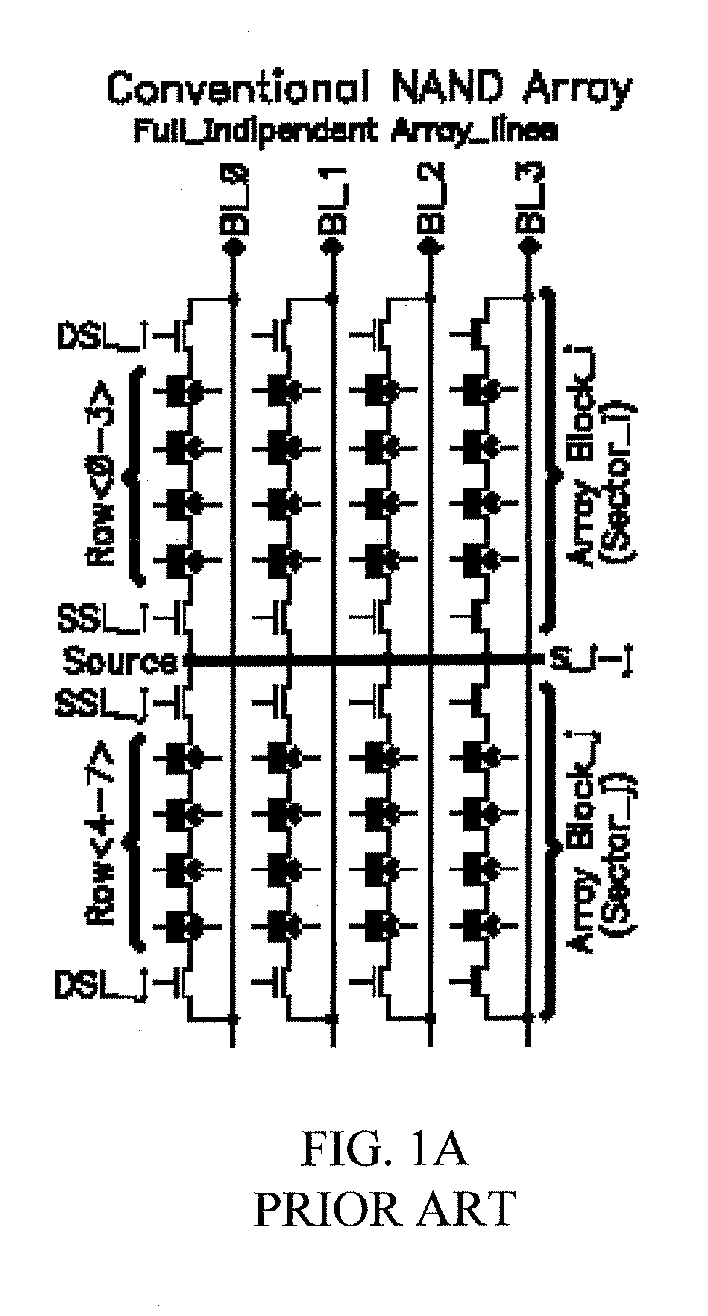
[0061] The device 20 incorporates at least one matrix 21 of memory cells organized in rows or word lines WL and columns or bit lines BL. The device 20 is however a memory of the Flash EEPROM type with a NAND architecture. FIGS. 6 and 8 show instead two possible implementations of the array relative to the fast sections 23a and 24a of Flash EEPROM memory with NAND architecture of the device 20.

[0062] The memory allows, to the expense of a slight modification of the array of a NAND memory, to realize in a single chip, and thus with a single technology, a group of functions being typical of different memories and up to now obtained only by way of devices of different nature and structure. In other words, the device 20 is realized on a single ...


PUM

PropertyMeasurementUnit
random access timeaaaaaaaaaa

Abstract

A non-volatile memory electronic device is integrated on a semiconductor and is of the Flash EEPROM type with an architecture of the NAND type including at least one memory matrix divided into sectors being singularly erasable and organized in rows or word lines and columns or bit lines of memory cells. Advantageously, the matrix may include logic sectors wherein pairs of rows or word lines are electrically short-circuited and refer to a single biasing terminal, source terminals of the associated cells of each pair of rows associated with a same source select line referring to a corresponding biasing terminal, and at least one pair of independent drain select lines, each of the rows and of the lines being provided with metallization shunts to by-pass groups of bit lines and/or to speed up the propagation times of the biasing in the corresponding logic sector.

Description

FIELD OF THE INVENTION [0001] The present invention relates to a Flash EEPROM electronic memory device monolithically integrated on semiconductor and having a NAND architecture comprising at least one memory matrix organized in memory cell rows and columns. The invention also relates to a method for programming the above memory device with the NAND structure. BACKGROUND OF THE INVENTION [0002] It is known that the market for non-volatile memories, for example of the EEPROM or Flash EEPROM type, is currently growing significantly and the most promising applications relate to the “data storage” field. Until a few years ago, such a market almost exclusively involved the consumer field of digital cameras, with the associated memory cards, or the known USB keys which represented expansion mobile memories for personal computers. Therefore, the demand for these products by the consumer market was mainly addressed to flash memories of large capacity. [0003] This trend seems to be destined t...

Claims


Application Information

Patent Timeline
Patent Type & Authority Applications(United States)
IPC IPC(8): G11C16/04
CPCG11C16/0483G11C16/12Y10T29/49002G11C16/08G11C16/24G11C16/0408
Inventor PASCUCCI, LUIGIROLANDI, PAOLO
Owner MICRON TECH INC
Why Eureka
Try Eureka