Electrostatic nanolithography probe actuation device and method

Inactive Publication Date: 2006-10-12
THE BOARD OF TRUSTEES OF THE UNIV OF ILLINOIS
View PDF14 Cites 32 Cited by
  • Summary
  • Abstract
  • Description
  • Claims
  • Application Information

AI Technical Summary

Problems solved by technology

However, the resolution of conventional projection optical lithographic systems, still the most widely used in the microelectronics industry, is limited by optical diffraction.
While the resolution can be improved by using beam-based direct-writing tools w

Method used


Image

  • Electrostatic nanolithography probe actuation device and method
  • Electrostatic nanolithography probe actuation device and method
  • Electrostatic nanolithography probe actuation device and method

Examples


Embodiment Construction

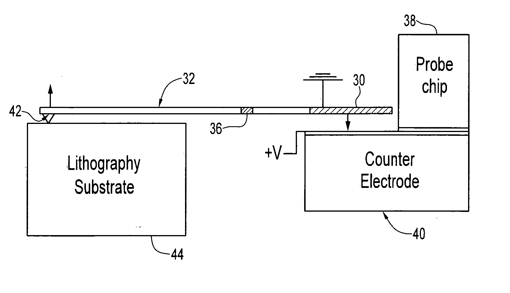
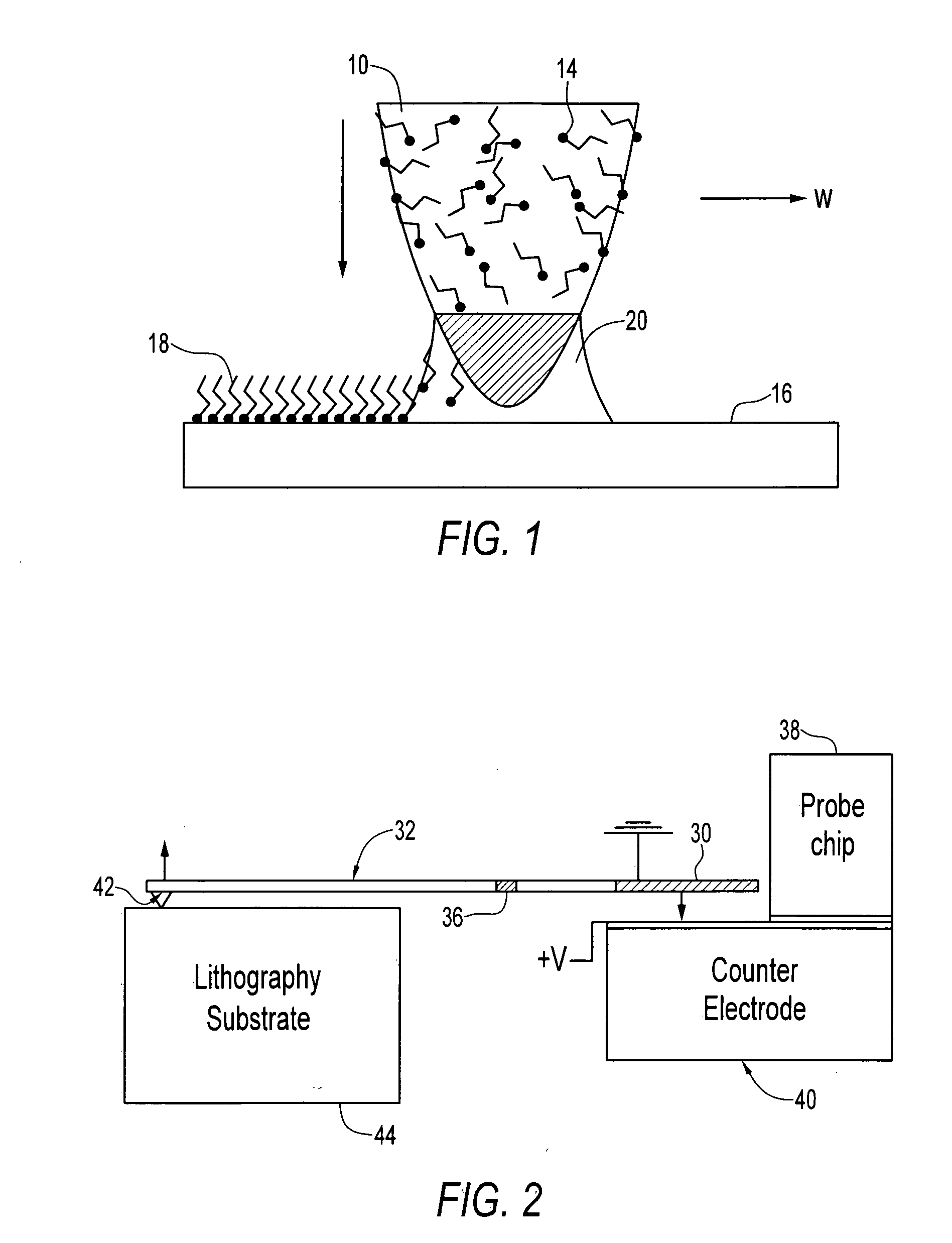
[0028] As disclosed in U.S. Pat. No. 6,642,129, one type of independent probe actuation method is electrostatic actuation. According to an embodiment of this method, motion in the probe is realized by providing a voltage difference between two opposing electrodes.

[0029] An example of electrostatic actuation as provided in U.S. Pat. No. 6,642,129 is shown in FIG. 2. A grounded, moveable probe electrode 30 is at an end of a probe 32, which may be part of a probe array. The probe 32 preferably is supported at or near its midpoint by a flexible suspension 36, such as a torsional spring. The flexible suspension 36 may be incorporated into a probe chip 38, for example. A second, stationary, electrode 40, which may also be incorporated into the chip 38, provides a counter electrode. A probe tip 42 is formed on a flexible end of the probe 32 longitudinally opposing the end including the probe electrode 30. At rest, the probe tip 42 preferably is placed in contact with a substrate 44 by pos...


PUM


Abstract

Method and apparatus for selectively actuating a cantilevered probe for applying a compound to a substrate in nanolithography. A probe having a probe electrode and a substrate having a counter electrode are provided. Voltage applied to the probe electrode and/or counter electrode provides electrostatic attraction between them, moving a probe tip into sufficient proximity to the substrate to apply the patterning compound. Alternatively, a flexible cantilevered probe anchored to a holder includes a layer of conductive material forming a probe electrode. A counter electrode on the holder faces the probe electrode. The holder and probe are positioned so that a probe tip applies the compound to the substrate. The probe is disposed between the substrate and the counter electrode. An electrostatic attractive force generated between the probe electrode and the counter electrode flexes the probe and lifts the tip away from the substrate to suspend writing.

Description

PRIORITY CLAIM [0001] This application is a continuation-in-part of U.S. patent application Ser. No. 11 / 073,938, which is a continuation of U.S. patent application Ser. No. 10 / 647,724, now U.S. Pat. No. 6,867,443, which is a divisional application of U.S. patent application Ser. No. 10 / 008,719, now U.S. Pat. No. 6,642,129, which claims the benefit of U.S. Provisional Application No. 60 / 307,976, under 35 U.S.C. § 119.STATEMENT OF GOVERNMENT INTEREST [0002] This invention was made with Government assistance under Contract Number DMD19-00-1-0414 and DAAD19-03-1-0065 awarded by the Defense Advanced Research Projects Agency (DARPA), and Award Number EEC-0118025 awarded by the National Science Foundation (NSF). The Government has certain rights in this invention.FIELD OF THE INVENTION [0003] A field of the present invention is nanotechnology. Another field of the present invention is nanolithography. Still other fields of the present invention include microfabrication and nanofabrication....

Claims


Application Information

Patent Timeline
IPC IPC(8): G12B21/02G01Q70/16G01Q80/00
CPCB82Y10/00B82Y40/00G01Q80/00B82Y35/00G01Q70/06G01Q70/16G03F7/0002
Inventor LIU, CHANGBULLEN, DAVID ANDREW
Owner THE BOARD OF TRUSTEES OF THE UNIV OF ILLINOIS
Why Eureka
Try Eureka