Image display device

a technology of image display and display device, which is applied in the direction of color television details, instruments, chemistry apparatus and processes, etc., can solve the problems of affecting the image quality of the image, and the technology does not provide a self-adjustment of the product itself, so as to reduce the adverse influence

Inactive Publication Date: 2006-10-19
HITACHI LTD
View PDF0 Cites 112 Cited by
  • Summary
  • Abstract
  • Description
  • Claims
  • Application Information

AI Technical Summary

Benefits of technology

[0007] According to the present invention, an optical sensor for detecting flickers is installed on a reflection mirror that serves to reflect a ray of light irradiated onto the display device installed in the image display device. Further, the optical sensor for detecting flickers may be located in a projecion lens unit. This location of the optical sensor

Problems solved by technology

That is, the technology does not provide a self-adjustment of the product itself.
Hence, this technology has difficulty in adjusting image quality degrade

Method used


Image

  • Image display device
  • Image display device
  • Image display device

Examples


first embodiment

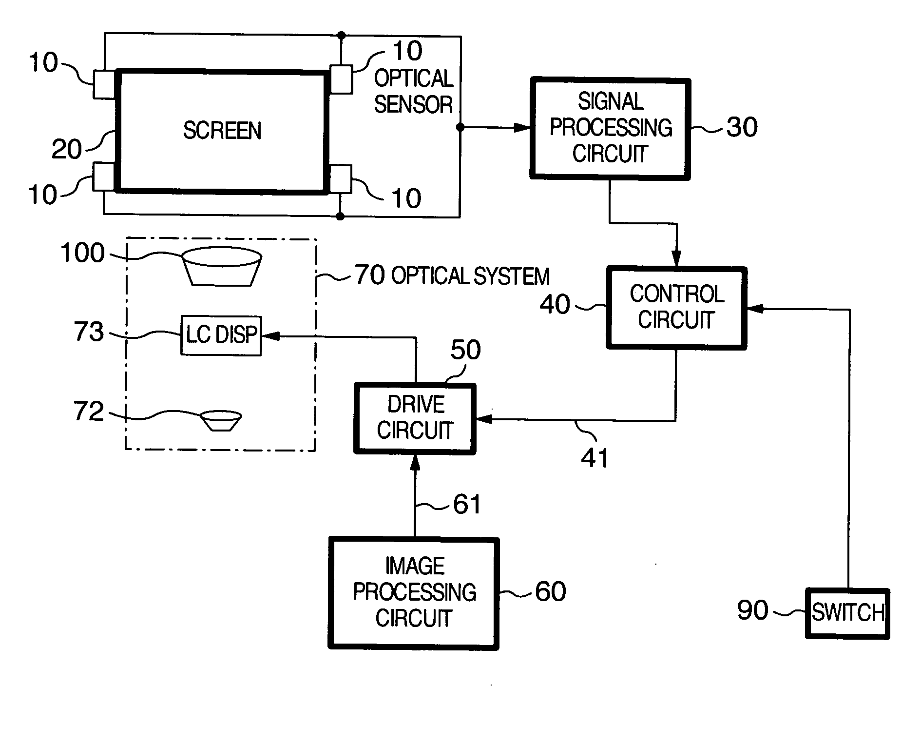
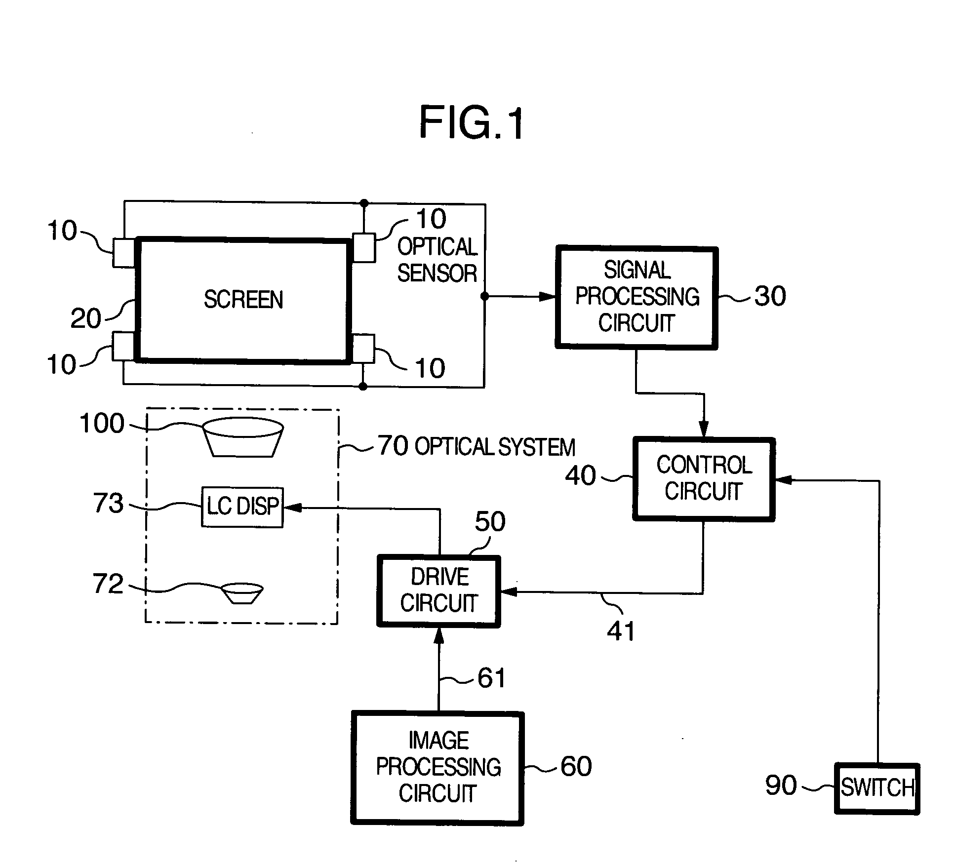
[0029]FIG. 1 is a block diagram showing a liquid crystal display device according to the first embodiment of the present invention. FIG. 4 shows a control flow of a control circuit included in the first embodiment. FIG. 7 is a block diagram showing a signal processing circuit included in the first embodiment.

[0030] In FIG. 1, the liquid crystal display device is arranged to have an image processing circuit 60, a drive circuit 50, an optical system 70, optical sensors 10, a signal processing circuit 30, a control circuit 40, and a switch 90. The image processing circuit 60 performs a predetermined image processing operation with respect to a video signal (not shown). The drive circuit 50 operates to drive a liquid crystal display device 73 based on the video signal 61 sent from the image processing circuit and a test pattern used for adjustment of flickers stored in an internal memory (not shown). The optical system 70 includes a light source 72, a liquid crystal display device 73 a...

second embodiment

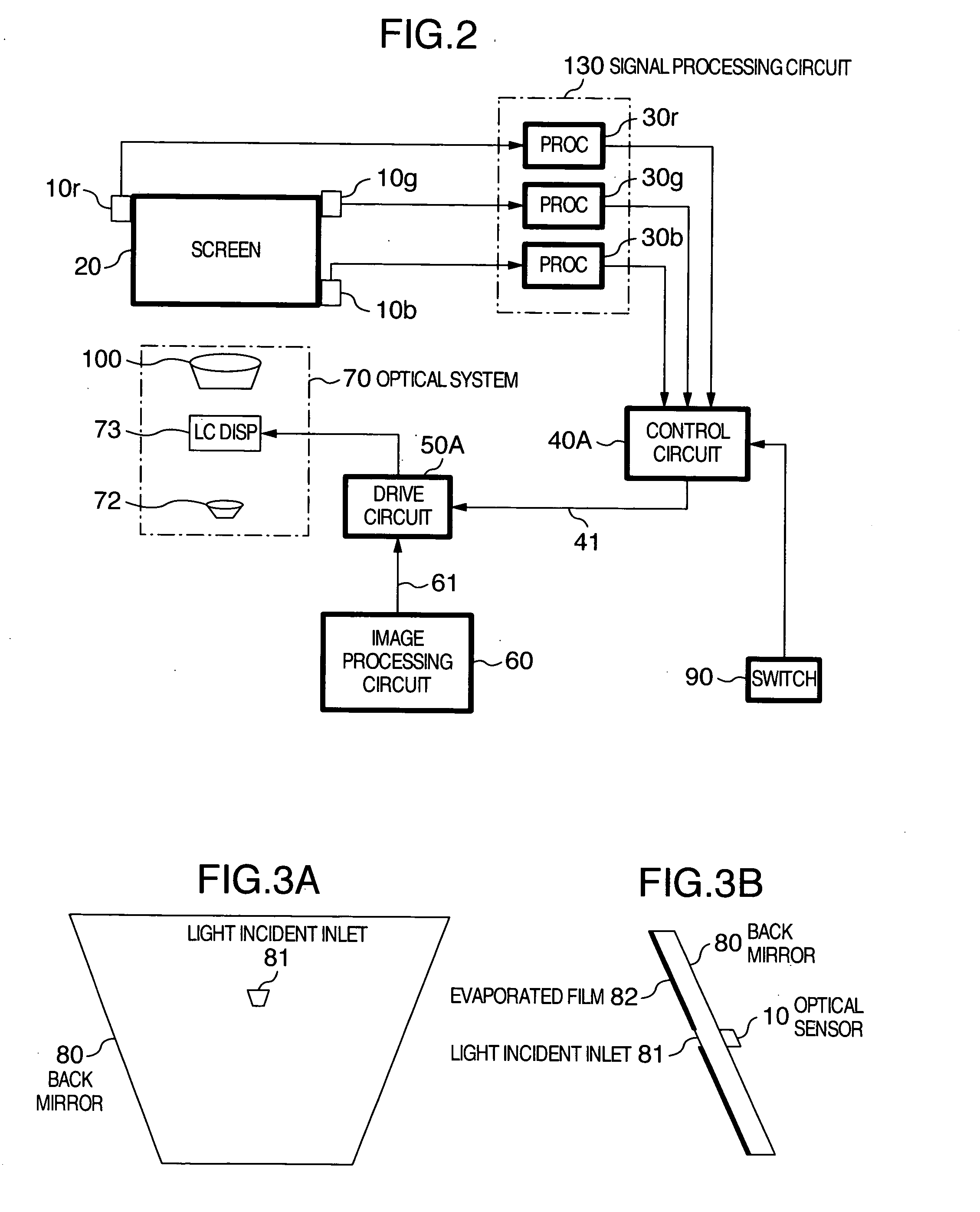
[0047] The first embodiment concerns with a serial adjusting process of serially carrying out the flicker adjustments of the liquid crystal display device corresponding with the first color (for example, the R color), the liquid crystal display device corresponding with the second color (for example, the G color), and finally the liquid crystal display device corresponding with the third color (for example, the B color). However, this serial adjustment process takes a considerably long time in completing all the flicker adjustments. Hence, the below-described second embodiment concerns with the flicker adjustment of each color at a time and in parallel for the purpose of reducing the adjustment time.

[0048]FIG. 2 is a block diagram showing a liquid crystal display device according to the second embodiment of the present invention. In FIG. 2, the components having the same functions as those shown in FIG. 1 have the same reference numbers and are not described for avoiding the duplic...

third embodiment

[0055] In the first and the second embodiments, the optical sensors 10 are located on the outer peripheral portion of the screen 20. However, the present invention is not limited to this location. In the first and the second embodiments, since the optical sensors are located on the outer peripheral portion of the screen, the quantity of light received by the optical sensors is small and the output signal amplitude of each optical sensor is also reduced. In the third embodiment, therefore, the optical sensor 10 is located on the rear of the back mirror (back-to-back mirror) used in the back projective type liquid crystal display device. This third embodiment will be described below.

[0056]FIGS. 3A and 3B are schematic diagram showing a back mirror that concerns with the third embodiment. FIG. 3A is an imaginary view provided when viewing the back mirror 80 from the front. FIG. 3B is an imaginary view provided when viewing the back mirror from the side.

[0057] In this embodiment, the ...


PUM


Abstract

An image display device is arranged to irradiate a ray of light from a light source into liquid crystal display devices, form an optical image corresponding with a video signal, and expansively project the optical image. The image display device includes a reflection mirror for reflecting the ray of light irradiated onto the liquid crystal display devices, an optical sensor being located on the reflection mirror and for detecting a light intensity, a drive circuit that causes the liquid crystal display devices to be driven, and a control unit that controls the drive circuit based on the light intensity detected by the optical sensor. In operation, the image display device provides a capability of adjusting a variable reference voltage of a common electrode brought about by variation with time ascribable to the liquid crystal display devices without preventing display of an input video signal.

Description

BACKGROUND OF THE INVENTION [0001] The present invention relates to an image display device which is arranged to expansively project an image appearing on display devices onto a screen for forming the expanded image on the screen. [0002] In the display devices of the image display device, for example, the active-matrix liquid crystal display devices (often called the liquid crystal display panel), an AC voltage to be reversed in a field or a line period is applied between a pixel electrode and a common electrode. However, the characteristic variation may take place in a transistor for driving the pixel electrode, so that the DC voltage applied onto the common electrode may be shifted from the reversed center voltage. As a result, flickers take place on the liquid crystal display devices. In order to prevent those flickers, the technology of automatically adjusting a reference voltage to be applied onto the common electrode before shippment has been proposed in JP-A-6-130920. [0003] ...

Claims


Application Information

Patent Timeline
IPC IPC(8): C09K19/34
CPCG09G3/002G09G2320/0247H04N9/3194H04N9/312H04N9/3182H04N9/3105
Inventor SAKAGUCHI, YOSHIHIROMAKINO, KAZUHITOIWASA, HIROSHIYOSHIZAWA, KAZUHIKOYOSHIDA, HIDEKI
Owner HITACHI LTD
Why Eureka
Try Eureka