High-Frequency, High-Signal-Density, Surface-Mount Technology Footprint Definitions

a technology of high signal density and definition, applied in the field of high signal density and surface mount technology footprint definition, can solve the problems of generated footprint and anticipated performance data to be updated, and achieve the effect of limiting cross-talk and increasing signal contact density

Active Publication Date: 2006-10-19
FCI AMERICAS TECH LLC
View PDF9 Cites 7 Cited by
  • Summary
  • Abstract
  • Description
  • Claims
  • Application Information

AI Technical Summary

Benefits of technology

[0014] The invention provides circuit board, such as backplane or printed circuit boards, for example, for receiving an electrical component having a contact arrangement of electrically conductive contacts. The circuit board may include an arrangement of vias and SMT pads that may be different from the contact arrangement. Terminal ends of the contacts housed by such a connector may be jogged or bent to electrically connect with the SMT pads on the circuit board. The SMT pads and vias may be arranged in a number of ways that allow for increased signal contact density, while limiting cross-talk among signal conductors and providing adequate space for routing of traces on the circuit board.

Problems solved by technology

The user may change the input data, thus causing the generated footprint and anticipated performance data to be updated accordingly.

Method used


Image

  • High-Frequency, High-Signal-Density, Surface-Mount Technology Footprint Definitions
  • High-Frequency, High-Signal-Density, Surface-Mount Technology Footprint Definitions
  • High-Frequency, High-Signal-Density, Surface-Mount Technology Footprint Definitions

Examples


Embodiment Construction

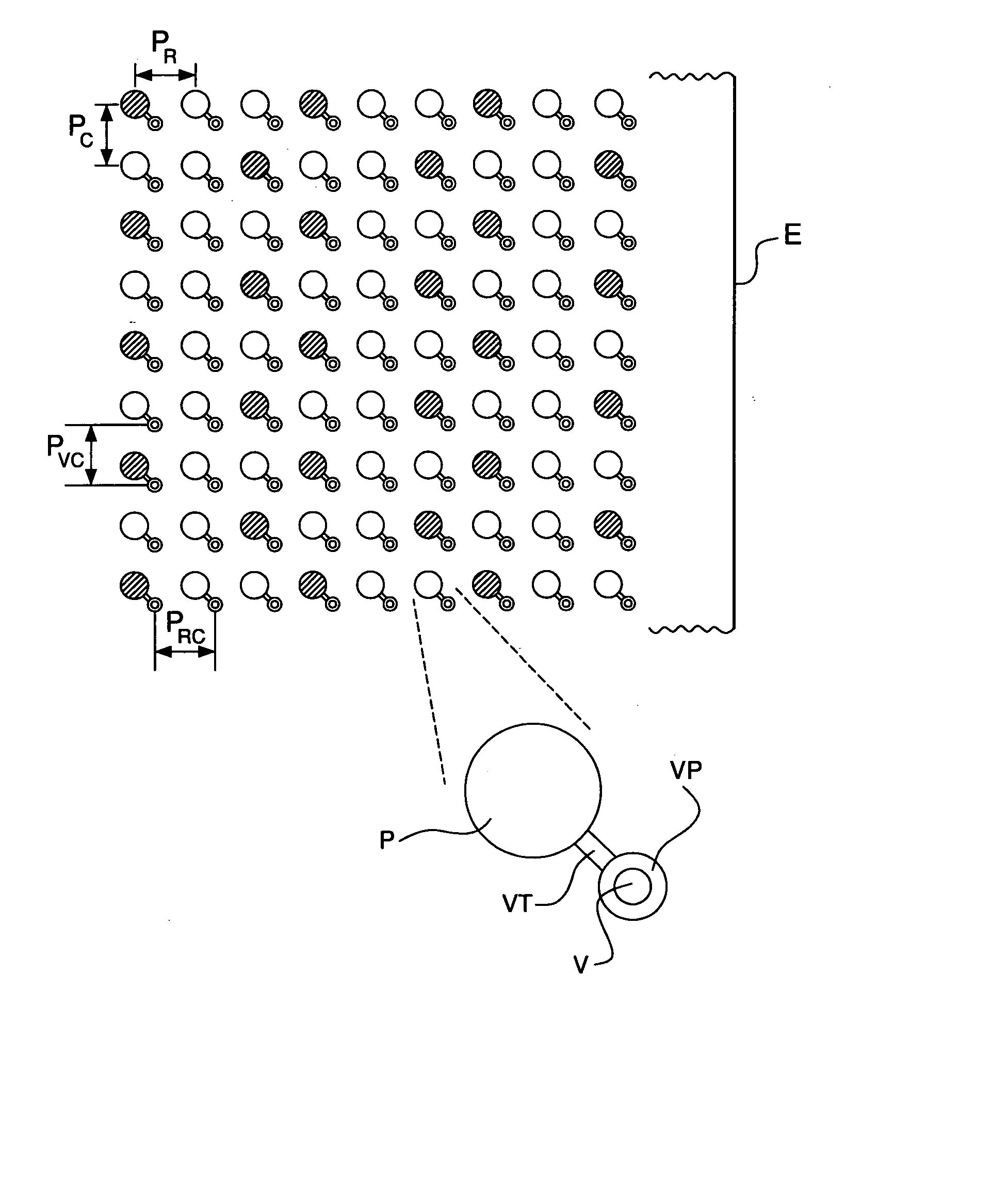
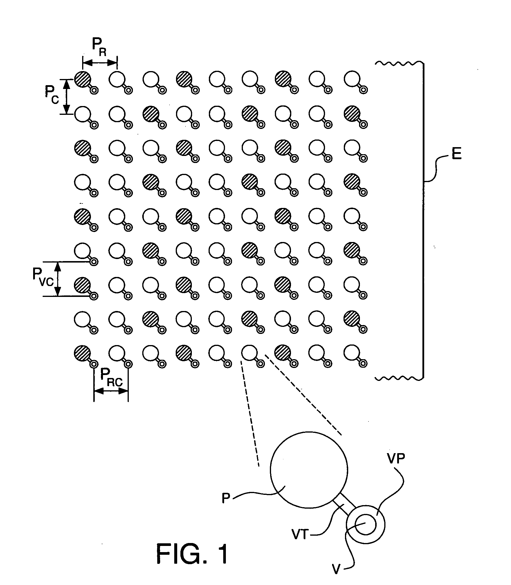
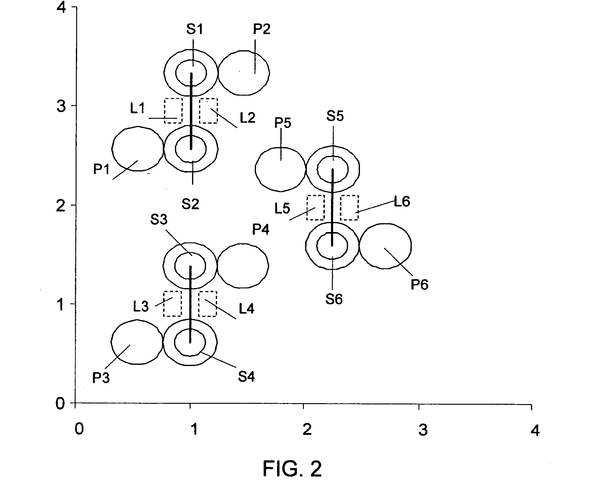
[0022]FIG. 2 depicts an example SMT connector footprint in accordance with an embodiment of the invention. As shown, the connector footprint may include a plurality of signal-conductor vias S1-S6 and a plurality of signal-conductor SMT pads P1-P6. The SMT pads and vias may be arranged in a so-called “dog-bone” pattern, such that each via is separate from, and electrically connected to, a respective SMT pad. In a typical dog-bone pattern, circuit board traces (not shown in FIG. 2) electrically connect the vias S1-S6 with respective ones of the SMT pads P1-P6. Alternatively, as described above, the vias and SMT pads may be arranged in a so-called “via-in-pad” arrangement.

[0023] The signal conductor vias may be used in either single-ended or differential transmission. In differential signal transmission, each signal conductor via may be paired with an adjacent signal conductor via. Via pairs are illustrated in FIG. 2 by a line connecting paired vias. If the connector to be received by...


PUM


Abstract

Methods for designing SMT connector footprints are disclosed. A circuit board may have disposed thereon an arrangement of SMT pads and corresponding vias. The arrangement of vias may differ from the arrangement of SMT pads. The arrangement of SMT pads may differ from the arrangement of contacts in a connector the footprint is designed to receive. The terminal ends of the contacts may be jogged or bent for electrical connection with the SMT pads. The SMT pads and vias may be arranged in a number of ways that increase signal contact density of the board, while limiting cross-talk and providing adequate impedance and routing space on the board. An interactive tool for designing such a footprint is disclosed.

Description

CROSS-REFERENCE TO RELATED APPLICATIONS [0001] This application claims benefit under 35 U.S.C. § 119(e) of provisional U.S. patent application No. 60 / 631,499, filed Nov. 29, 2004. [0002] This application is related to U.S. patent application Ser. No. [attorney docket FCI-2878 (C3716)], filed [on even date herewith and entitled “Improved Matched-Impedance Surface-Mount Technology Footprints”], to provisional U.S. patent application No. 60 / 631,545, filed Nov. 29, 2004, and to provisional U.S. patent application No. 60 / 686,514, filed Jun. 1, 2005. [0003] The contents of each of the above-referenced U.S. patent applications is incorporated herein by reference.FIELD OF THE INVENTION [0004] Generally, the invention relates to electrical connector / circuit board systems. More particularly, the invention relates to methodologies for defining high-frequency, high-signal-density, surface-mount-technology footprints on such circuit boards. BACKGROUND OF THE INVENTION [0005] Typically, an electr...

Claims


Application Information

Patent Timeline
Patent Type & Authority Applications(United States)
IPC IPC(8): H01L23/58
CPCH05K1/0237H05K1/114H05K2201/10734H05K2201/09236H05K2201/10189H05K3/0005
Inventor WININGS, CLIFFORD L.SHUEY, JOSEPH B.
Owner FCI AMERICAS TECH LLC
Why Eureka
Try Eureka