WOA panel architecture

a technology of liquid crystal display and panel, applied in the direction of instruments, computing, electric digital data processing, etc., can solve the problems of increasing yield and profit, and achieve the effects of reducing the cost of the fpc, and reducing the size of the pcb

Inactive Publication Date: 2006-10-19
HIMAX TECH LTD
View PDF14 Cites 79 Cited by
  • Summary
  • Abstract
  • Description
  • Claims
  • Application Information

AI Technical Summary

Benefits of technology

[0016] Certain embodiments of the present invention utilize WOA technology, which eliminates the cost of FPCs. The size of the PCB can be reduced due to the omission of the connection area for the FPCs, the reduction in size being proportional to the number of...

Problems solved by technology

This can also inc...

Method used


Image

  • WOA panel architecture
  • WOA panel architecture
  • WOA panel architecture

Examples


Embodiment Construction

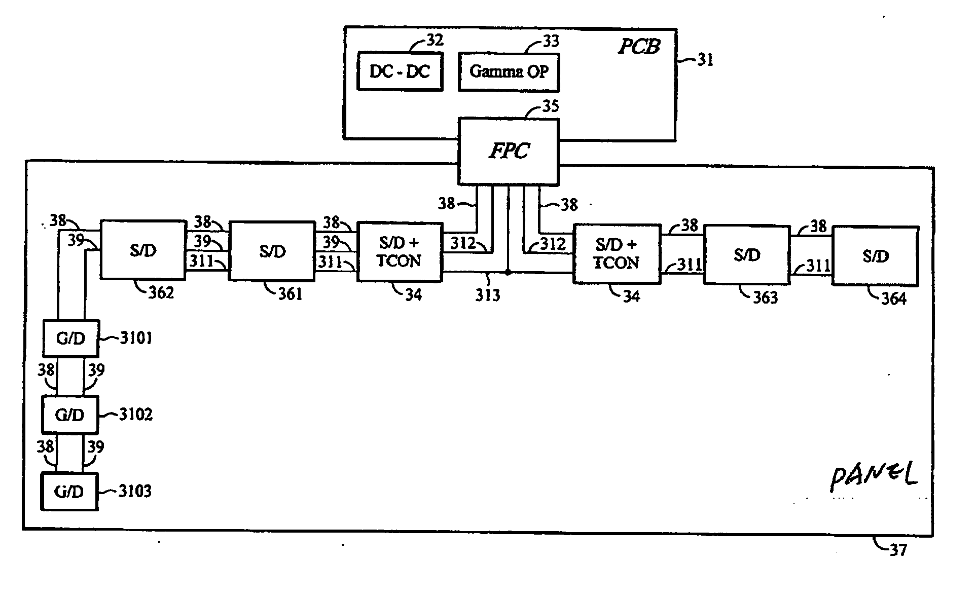
[0036]FIG. 3 illustrates a wiring-on-array (“WOA”) panel architecture according to certain embodiments of the present invention. The panel architecture, comprises a display panel 37, a PCB 31 coupling the display panel 37 with an FPC 35, a PCB 31 comprising a DC-to-DC converter IC (DC-DC) 32 to provide power, and a gamma operational amplifier IC (Gamma OP) 33 to provide gamma reference voltage signals. The panel architecture further comprises a plurality of source driver ICs (S / D) 361-364 and a plurality of gate driver ICs (G / D) 3101-3103 mounted on the display panel 37 using a COG process, and at least one integrated chip 34 mounted on the display panel 37 that performs the functions of both a source driver IC (S / D) 361 and a timing controller.

[0037] The COG process allows a chip to be positioned directly on a display panel. This can be achieved by using gold bumps grown on the driver ICs and the use of ACF (Anisotropic Conductive Film) material. Typically, the pads on standard ch...


PUM


Abstract

The present invention provides solutions to simplify and reduce the resources needed for manufacturing liquid crystal display modules. Failure of mid-process steps during mass production can result in significant costs. According to certain embodiments of the present invention, a WOA display panel architecture requires fewer LCM resources or has no PCB. Although the COG process and WOA method provide higher reliability in temporary LCD production, the costs associated with the space required for wires on the PCB or display panel for larger panel sizes remains expensive. Larger panel sizes also requires an increased number of driver ICs to construct a flat display panel. Similarly, the number of wires connecting each driver IC to a timing controller IC, gamma operational amplifier IC and DC-to-DC converter IC creates spacing problems that translate into higher production costs. These problems can be solved by certain embodiments of the present invention.

Description

CROSS-REFERENCE TO RELATED APPLICATION [0001] This application claims the benefit of U.S. Provisional Application Ser. No. 60 / 671,355, filed Apr. 14, 2005, pursuant to 35 U.S.C. § 119(e), which application is hereby incorporated by reference.FIELD OF THE INVENTION [0002] The present invention relates to a liquid crystal display (LCD) apparatus for displaying images, and in particular certain embodiments of the present invention relate to an architecture of an LCD device allowing the costs associated with liquid crystal display module (LCM) resources to be reduced. BACKGROUND OF THE INVENTION [0003] Now that people are accustomed to liquid crystal display (LCD) devices, the applications of LCD are expanding, forcing the manufacture of LCD devices to become a cost effective industry. Liquid crystal display module (LCM) production includes producing a glass panel, packaging driver chips with a chip on glass (COG) process, attaching a flexible printed circuit board (FPC) to the glass, a...

Claims


Application Information

Patent Timeline
IPC IPC(8): G09G5/00
CPCG09G2300/0426G09G3/3611
Inventor CHEN, YING-LIEHWU, BIING-SENGBU, LIN-KAI
Owner HIMAX TECH LTD
Why Eureka
Try Eureka