Dual wavelength thermal flux laser anneal

a laser annealing and thermal flux technology, applied in the direction of laser beam welding apparatus, welding apparatus, manufacturing tools, etc., can solve the problems of increasing the thermal budget required for thermal processing, drastically reducing the thermal budget, and even spike annealing becoming insufficient for advanced processing

Active Publication Date: 2006-10-19
APPLIED MATERIALS INC
View PDF12 Cites 46 Cited by
  • Summary
  • Abstract
  • Description
  • Claims
  • Application Information

AI Technical Summary

Benefits of technology

[0018] The heating beam may effectively radiate the sample at angles near 40° off normal.

Problems solved by technology

Such long periods at elevated temperatures substantially increase the thermal budget required for thermal processing.
A typical RTP heat-up rate is about 250° C. / s and a typical RTP cool-down rate is about 90° C. / s, thus drastically reducing the thermal budget.
However, the cooling and heating rates of RTP and even spike annealing are becoming insufficient for advanced devices having ultra-narrow features and shallow and abrupt junctions, both of which require precise thermal control.
The radiative cooling becomes less effective as the wafer cools.
Pulsed laser thermal processing, however, presents uniformity problems arising in part from the short, intense radiation pulses on a patterned surface.
The radiation pulse is so short that any difference in absorption will result in a large difference in temperature.
Diode lasers, however, suffer several drawbacks.
Laser bars create a problem in focusing their output into a beam uniform along its length.
That is, the linear uniformity at the laser source is not good and needs to be improved by an homogenizer.
The technology for homogenizers is available, but applying them to high intensity beams presents engineering and operational problems.
A further problem is that laser bar radiation at 808 nm has an absorption depth of about 800 nm in silicon, which may be greater than the depth of the silicon layer requiring annealing, such as shallow source and drain implants needing implant curing and dopant activation.
Although CO2 lasers have a lower efficiency (10 to 15%) than diode lasers (40 to 50%), they can more easily produce a well collimated (non-divergent) and generally circular beam, we believe that CO2 radiation having a wavelength of about 10.6 μm is ineffective as the sole source of laser radiation since the 10.6 μm wavelength is much greater than the silicon bandgap wavelength of 1.11 μm.
As a result, undoped or low-temperature silicon is virtually transparent to CO2 radiation and the CO2 is not effectively absorbed in a silicon wafer, more or less its shallow surface region desired for advanced microprocessing.
However, the heating apparatus complicates the laser thermal processing apparatus, and the doping levels cannot be freely controlled in semiconductor fabrication and vary across the partially developed integrated circuit.
Boyd does not address the spatial extent of his beams and admits to poor spatial definition, issues that are crucial for advanced laser thermal processing.

Method used


Image

  • Dual wavelength thermal flux laser anneal
  • Dual wavelength thermal flux laser anneal
  • Dual wavelength thermal flux laser anneal

Examples


Embodiment Construction

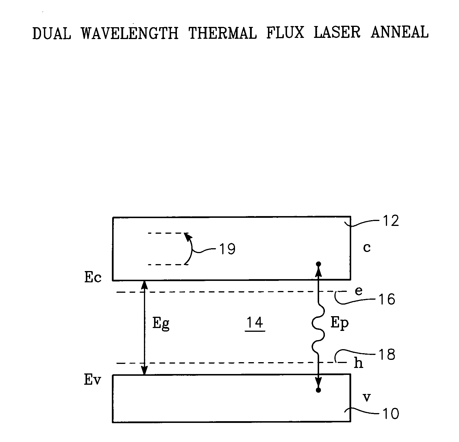
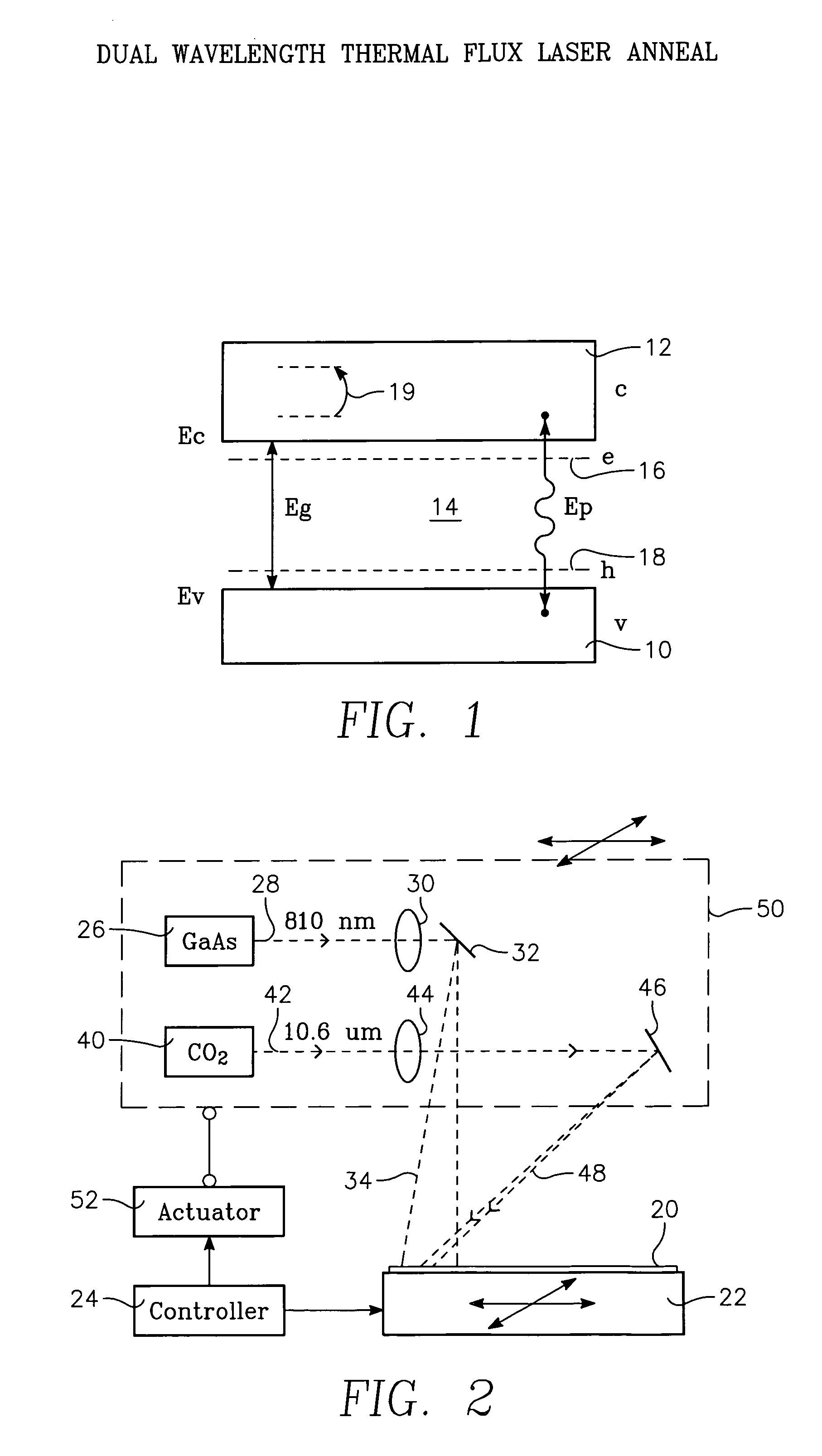
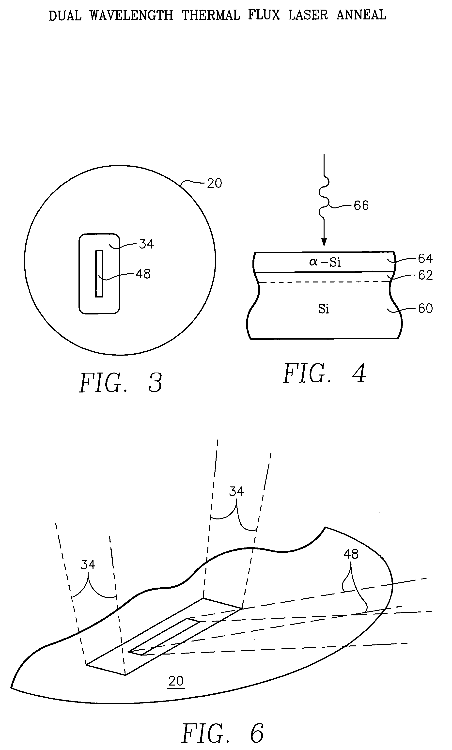
[0029] A simplified representation of one embodiment of the invention is schematically illustrated in the elevational view of FIG. 2. A wafer 20 or other substrate is held on a stage 22 that is motor driven in one or two directions under the control of a system controller 24. A short-wavelength laser 26, such as a GaAs laser bar, emits a visible or nearly visible continuous wave (CW) beam 28 at a wavelength which is shorter than the silicon bandgap wavelength of about 1.11 μm. For the GaAs laser 26, the emission wavelength is typically about 810 nm, which can be characterized as red. First optics 30 focus and shape the beam 28 and a reflector 32 redirects the beam 28 towards the wafer 20 in a relatively wide activating beam 34, also illustrated in the plane view of FIG. 3. The activating beam 34 may be inclined at some angle, for example, of 15° with respect to the wafer normal to prevent reflection back to the GaAs laser 26, which may shorten the lifetime of diode lasers. A long-wa...


PUM

PropertyMeasurementUnit
wavelengthaaaaaaaaaa
temperatureaaaaaaaaaa

Abstract

A thermal processing apparatus and method in which a first laser source, for example, a CO2 emitting at 10.6 μm is focused onto a silicon wafer as a line beam and a second laser source, for example, a GaAs laser bar emitting at 808 nm is focused onto the wafer as a larger beam surrounding the line beam. The two beams are scanned in synchronism in the direction of the narrow dimension of the line beam to create a narrow heating pulse from the line beam when activated by the larger beam. The energy of GaAs radiation is greater than the silicon bandgap energy and creates free carriers. The energy of the CO2 radiation is less than the silicon bandgap energy so silicon is otherwise transparent to it, but the long wavelength radiation is absorbed by the free carriers.

Description

FIELD OF THE INVENTION [0001] The invention relates generally to thermal processing of semiconductor substrates. In particular, the invention relates to laser thermal processing of semiconductor substrates in which a line beam is scanned across the substrate. BACKGROUND ART [0002] The fabrication of semiconductor integrated circuits has long required multiple steps of thermal processing a silicon wafer or other semiconductor wafer. The wafer may need to be raised to a temperature of 600° C. or well above to thermally activate a process. Such processes, though not so limited, may include chemical vapor deposition, silicidation, oxidation or nitridation, implant anneal, and dopant activation among others. Some of these processes may require temperatures in excess of 1000° C., 1200° C., or even above 1350° C., the last of which is relatively close to the melting point 1416° C. of silicon. [0003] Such thermal processing was originally performed in ovens typically containing many wafers ...

Claims


Application Information

Patent Timeline
Patent Type & Authority Applications(United States)
IPC IPC(8): H01L21/336
CPCB23K26/0066B23K26/0604B23K26/0608B23K26/0613B23K26/0732B23K26/073B23K26/0738H01L21/2026H01L21/324H01L21/268B23K26/0736B23K26/352H01L21/02675H01L21/02532
Inventor JENNINGS, DEANLIANG, HAIFANYAM, MARKPARIHAR, VIJAYMAYUR, ABHILASH J.HUNTER, AARONADAMS, BRUCERANISH, JOSEPH MICHAEL
Owner APPLIED MATERIALS INC
Why Eureka
Try Eureka