Dielectric antenna for high frequency wireless communication apparatus

a high-frequency wireless communication and dielectric antenna technology, applied in the direction of antenna details, antennas, electrically long antennas, etc., can solve the problems of deteriorating radio wave radiation characteristics, affecting the efficiency of radio wave radiation transmission, and consuming or occupying substantial space, so as to achieve efficient and economic prevention of a drop in the efficiency of radio wave radiation, and the effect of eliminating impedance mismatch

Inactive Publication Date: 2006-02-07
NGK SPARK PLUG CO LTD
View PDF29 Cites 54 Cited by
  • Summary
  • Abstract
  • Description
  • Claims
  • Application Information

AI Technical Summary

Benefits of technology

[0008]It is an object of the invention to provide a dielectric antenna which is capable of eliminating impedance mismatching resulting from miniaturization of the antenna without the addition of a special matching circuit, and which is thus capable of efficiently and economically preventing a drop in the efficiency of radiation of radio waves, resulting from impedance mismatches.
[0010]In this embodiment, formation of the conductive taper layer effectively achieves impedance matching without affecting the space savings provided by miniaturization of the antenna, and provides excellent radio wave radiation characteristics.
[0011]In accordance with another aspect of the invention, the dielectric antenna comprises first and second conductor portions formed on a dielectric substrate of the antenna and electrically connected to each other through a connection conductor portion having a tapered shape that expands in width at a predetermined taper angle from the first conductor portion side towards the second conductor portion side. When the taper angle of this connection conductor portion is 5° to 70° (preferably 8° to 68° and, more preferably, 10° to 60°), the antenna suppresses impedance mismatching and efficiently radiates the high frequency signals.
[0013]In this aspect of the invention, the impedance mismatch caused by the difference in specific dielectric constant between the dielectric substrate on which the feed strip is formed and the dielectric substrate on which the antenna comprising the meander line layer is formed is effectively eliminated by the provision of the extended feed line.
[0015]According to yet another aspect of the invention, various dimensional factors and relationships relating to the meander antenna line are provided which improve the performance of the dielectric antenna.

Problems solved by technology

An antenna is an indispensable constituent element in wireless communication but has the disadvantage of consuming or occupying substantial space, relatively speaking.
Moreover, impedance mismatching with the line on the component packaging substrate is more likely to occur, thereby resulting in deterioration of the radio wave radiation characteristics.
In other words, it is more difficult to efficiently transmit the high frequency signals supplied from a feed terminal to the antenna line.
However, given ever more demanding space requirements, i.e., due to the need for miniaturization, the antenna line length cannot always be arbitrarily changed.
Further, while it is known to insert a matching circuit between the line on the component packaging substrate side and the antenna line, the addition of such a matching circuit tends to increase production costs and to consume excessive space, which is, of course, contrary to the need for miniaturization.
There are various factors causing impedance mismatching between the antenna line and the feed terminal portion.
For instance, when, due to design limitations, the antenna line width is different from the width of a feed strip line for signal transmission, and particularly when the width of the antenna line is smaller than that of the feed strip due to miniaturization of the antenna, a problem with impedance mismatching is most likely to occur.

Method used


Image

  • Dielectric antenna for high frequency wireless communication apparatus
  • Dielectric antenna for high frequency wireless communication apparatus
  • Dielectric antenna for high frequency wireless communication apparatus

Examples


Embodiment Construction

[0031]An embodiment according to a first aspect of the invention will be explained with reference to the drawings, and in particular, in relation to FIG. 1.

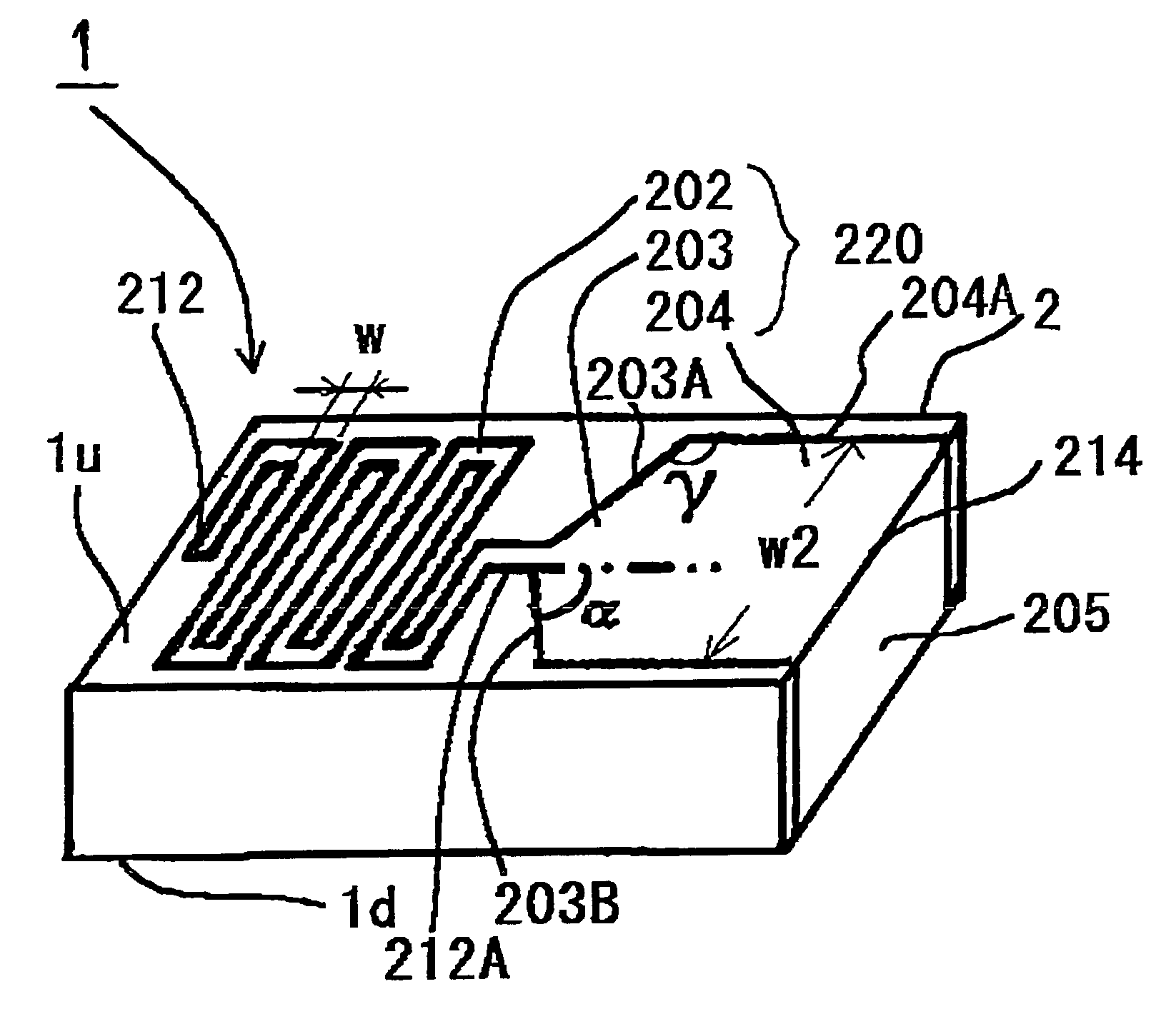
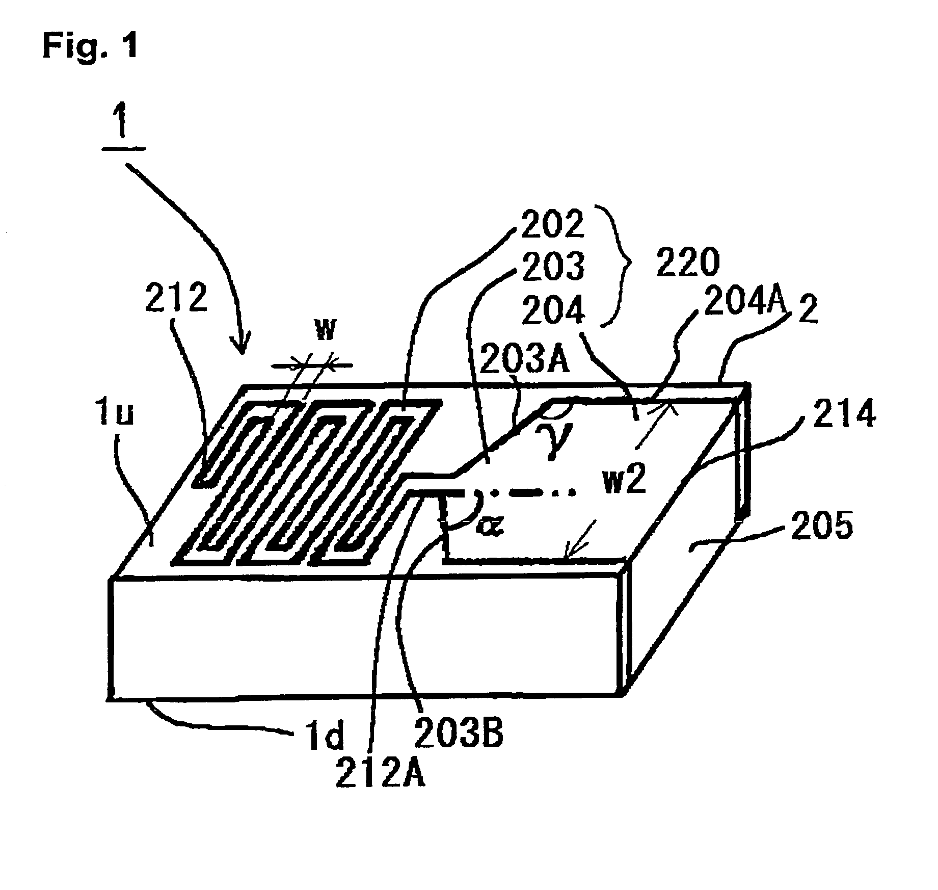
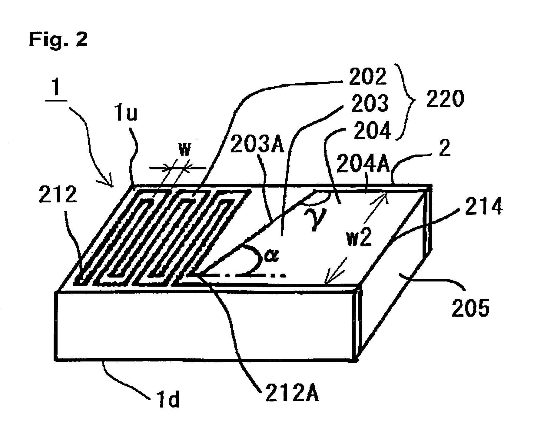
[0032]Referring to FIG. 1, a dielectric antenna 1 includes a dielectric substrate 2 typically made of alumina ceramic and having a rectangular solid shape, and a conductor portion 220 typically formed of Ag baked on one of the main surfaces 1u of the dielectric substrate 2. The conductive portion 220 comprises a conductive meander line layer or element 202, and a conductive feed line layer or element 204 and a conductive taper layer or element 203. The taper layer 203 connects one end of the meander line layer 202 to the feed line layer 204, and has an edge 203A thereof which is slanted with respect to, i.e., is inclined an angle to, an adjoining edge 204A of the feed line layer 204 in a direction toward the meander line layer 202. An angle γ of 110°–175°, and more preferably 120°–170°, is formed between the edges. The other end ...


PUM


Abstract

A dielectric antenna is provided for a high frequency wireless communication apparatus. The antenna includes a dielectric substrate and a conductive meander line layer formed on the dielectric substrate. A conductive feed line layer, having a greater line width than the width of the meander line layer, is also formed on the dielectric substrate. A conductive taper layer connects the conductive meander line layer to the conductive feed line layer. An edge of the conductive taper layer slants at an angle from an adjacent edge of the conductive feed line layer in a direction toward the conductive meander line layer.

Description

BACKGROUND OF THE INVENTION[0001]1. Field of the Invention[0002]This invention relates to an antenna in use for wireless communication, and in particular, to a dielectric antenna having a so-called meander line configuration formed on a dielectric substrate for use in high frequency wireless communication.[0003]2. Related Art[0004]An antenna is an indispensable constituent element in wireless communication but has the disadvantage of consuming or occupying substantial space, relatively speaking. To reduce the size of the antenna, known antenna configurations use a dielectric material and form an antenna line on or within the dielectric material. An example of antennas according to this prior art is described in Japanese Patent Laid-Open No. 13126 / 1998. To suppress or reduce exothermy (heat evolution) resulting from a power loss from a radiation electrode and to provide an antenna having reduced wavelength fluctuation, the antenna has a construction as shown in FIG. 13. Referring to ...

Claims


Application Information

Patent Timeline
Patent Type & Authority Patents(United States)
IPC IPC(8): H01Q1/38H01Q11/14
CPCH01Q11/14H01Q1/38
Inventor SUGIMOTO, NORIYASUKANAMORI, TAKASHINAKATA, DAISUKEWAKAMATSU, SUSUMUTAKADA, TOSHIKATSU
Owner NGK SPARK PLUG CO LTD
Why Eureka
Try Eureka