Multi-domain vertical alignment liquid crystal display and driving method thereof

a liquid crystal display and vertical alignment technology, applied in static indicating devices, instruments, non-linear optics, etc., can solve the problems of color shift and color washout, and the requirement for longer response time, so as to shorten the response time and eliminate the effect of color washout in accordance with the viewing angle chang

Active Publication Date: 2006-10-26
AU OPTRONICS CORP
View PDF7 Cites 23 Cited by
  • Summary
  • Abstract
  • Description
  • Claims
  • Application Information

AI Technical Summary

Benefits of technology

[0024] In summary, adoption of DDEs in the present invention not only solves the problem of light leakage, but also pre-tilts the liquid crystal molecules for shortening the response time required. Furthermore, according to the present invention, two effective voltages are applied to the liquid crystal layer over a same pixel unit; therefore, the problems of color shift and color washout in accordance with the viewing angle changes can be eliminated.

Problems solved by technology

In other words, as the viewing angle changes, the conventional MVA-LCD panel may display a luminance change accordingly, which may further cause a color shift and a color washout.
Also, the employment of alignment protrusions may cause a light leakage, and using slits may lead to a requirement for longer response time.

Method used


Image

  • Multi-domain vertical alignment liquid crystal display and driving method thereof
  • Multi-domain vertical alignment liquid crystal display and driving method thereof
  • Multi-domain vertical alignment liquid crystal display and driving method thereof

Examples


first embodiment

[0038] The First Embodiment

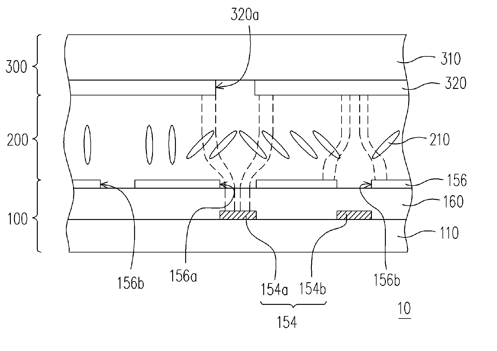
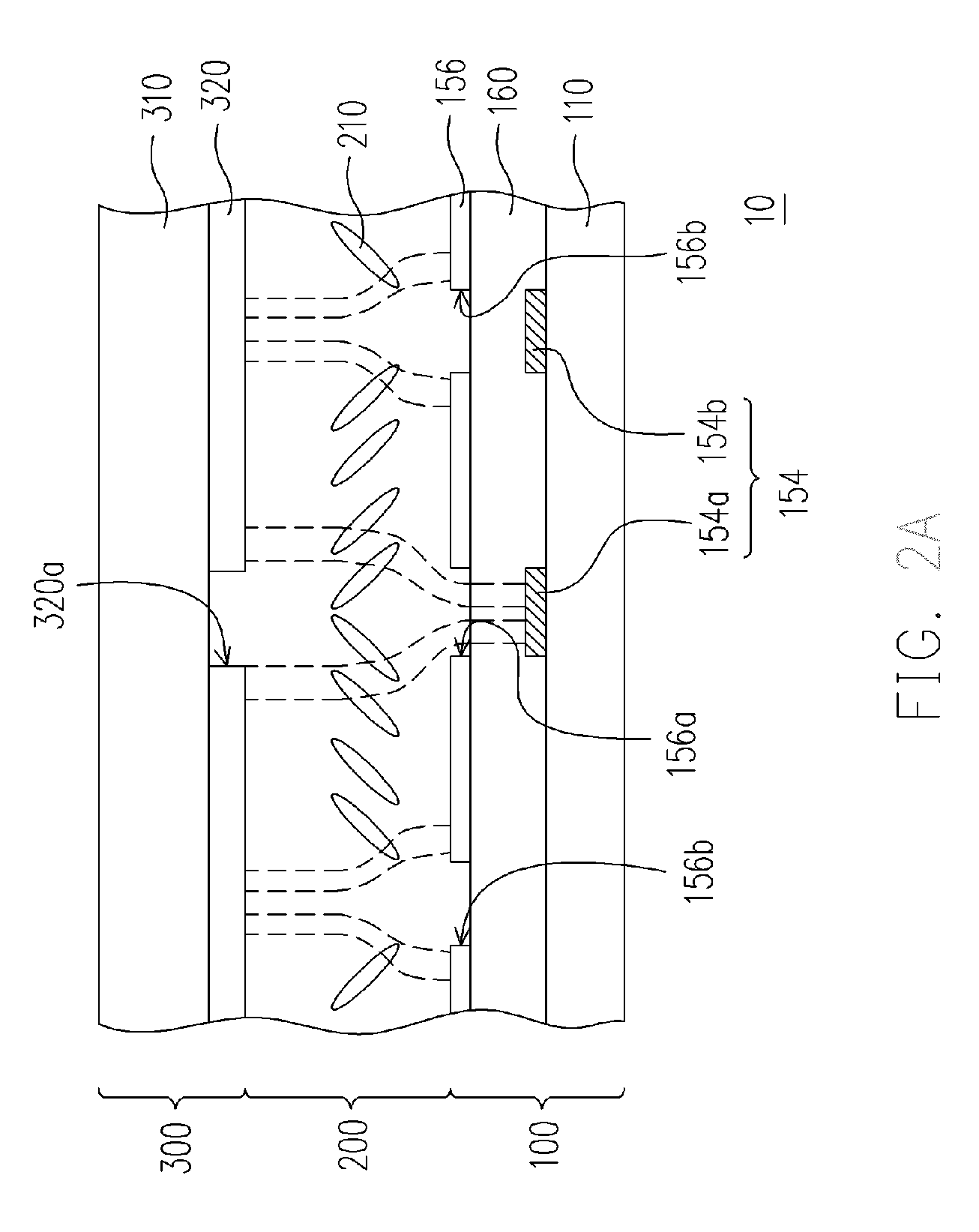
[0039]FIG. 2A is a cross-sectional view of an MVA-LCD panel according to the first embodiment of the present invention and FIG. 2B is a view from the top of the active components array substrate of FIG. 2A. Referring to FIGS. 2A and 2B, a MVA-LCD panel includes an active component array substrate 100, an opposite substrate 300 and a liquid crystal layer 200. The liquid crystal layer 200 is disposed between the active component array substrate 100 and the opposite substrate 300.

[0040] The active component array substrate 100 can be a thin film transistor (TFT) array substrate, a diode array substrate or other active component array substrates, while the opposite substrate 300 for example can be a color filter substrate. However, the active component array substrate 100 can also be a color filter on array (COA) substrate, while the opposite substrate 300 is an upper substrate having common electrodes. The COA substrate has a structure of a TFT array substra...

second embodiment

[0052] The Second Embodiment

[0053]FIG. 5A is a cross-sectional view of an MVA-LCD panel according to the second embodiment of the present invention. FIG. 5B is a view of the opposite substrate of FIG. 5A from the liquid crystal side. Referring to FIGS. 5A and 5B, both of which use two pixels (upper and lower) as example for illustration, while it may apply in a display panel containing one or multiple pixel units. According to the embodiment of the MVA-LCD panel 20, the common electrode layer 410 of the opposite substrate 400 includes a plurality of common electrode sets 412, 414 and 416, and the common electrode sets are insulated from each other. Further, each of the common electrode sets 412, 414 and 416 includes a plurality of common electrodes; however, only the adjacent two upper and lower pixel electrodes are illustrated as an example according to FIG. 5B, herein the common electrode sets 412, 414 and 416 respectively include two, two and one common electrodes. In this embodi...

third embodiment

[0063]FIG. 8 is a cross-sectional view of an MVA-LCD panel according to the present invention. Referring to FIG. 8, in an MVA-LCD panel 30 according to the embodiment, an opposite substrate 500 has a common electrode layer 510 facing toward the active component array substrate 100. A dielectric layer 600 covers a part of the common electrode layer 510 and a part of the pixel electrode 156. It should be noted that the dielectric layer 600 may also cover a part of the common electrode layer 510 only or cover a part of the pixel electrode 156 only.

[0064] More specifically, the dielectric layer 600 may cover upon the slit 156b (shown at the two sides of FIG. 8) of the pixel electrode 156; and the dielectric layer 600 may also be disposed on the common electrode layer 510 (shown at the central part of FIG. 8) over the DDE 154. Furthermore, the material for forming the dielectric layer 600 can be transparent organic material or transparent inorganic material.

[0065] The dielectric layer 6...


PUM

PropertyMeasurementUnit
voltageaaaaaaaaaa
voltageaaaaaaaaaa
voltagesaaaaaaaaaa

Abstract

An MVA-LCD panel, including an active component array substrate, an opposite substrate and a liquid crystal layer disposed between is provided. The active component array substrate includes scan lines, data lines, control lines and pixel units. Each of the pixel units includes an active component, a domain division electrode (DDE) and a pixel electrode. The active component is electrically connected with the corresponding scan line and the corresponding data line, the DDE being electrically connected with the corresponding control line, the pixel electrode being electrically connected with the active component. The pixel electrode has first slits, and the first DDE are disposed under the first slits. The opposite substrate has a common electrode layer facing toward the active component array substrate. The common electrode layer includes second slits and at least a part of the second slits is disposed over the first domain division electrode.

Description

CROSS-REFERENCE TO RELATED APPLICATION [0001] This application claims the priority benefit of Taiwan application serial no. 94113064, filed on Apr. 25, 2005. All disclosure of the Taiwan application is incorporated herein by reference. BACKGROUND OF THE INVENTION [0002] 1. Field of the Invention [0003] The present invention relates to a liquid crystal display panel, and particularly to a multi-domain vertical alignment liquid crystal display (MVA-LCD) panel and a driving method thereof. [0004] 2. Description of Related Art [0005] Nowadays, a commercial thin film transistor liquid crystal display (TFT-LCD) is required to have the characteristics of high contrast ratio, no gray scale inversion, little color shift, high luminance, high color richness, high color saturation, rapid response and wide viewing angle. The conventional displays which can match the demand for wide viewing angle include twisted nematic (TN) LCD displays with wide viewing films, in-plane switching (IPS) LCD disp...

Claims


Application Information

Patent Timeline
Patent Type & Authority Applications(United States)
IPC IPC(8): G02F1/1337
CPCG02F1/133707G02F1/134309G02F1/1393G09G2320/0252G09G3/3648G09G2300/043G09G2300/0439G02F2001/13373G02F1/13373
Inventor SU, JENN-JIA
Owner AU OPTRONICS CORP
Why Eureka
Try Eureka