Electrostatic chuck for track thermal plates

a technology of electrostatic chuck and thermal plate, which is applied in the direction of electrostatic holding device, manufacturing tools, contacts, etc., can solve the problems of increasing linewidth, affecting device performance, and not being able to remove portions of the photoresist layer as desired

Inactive Publication Date: 2006-10-26
SOKUDO CO LTD
View PDF20 Cites 13 Cited by
  • Summary
  • Abstract
  • Description
  • Claims
  • Application Information

AI Technical Summary

Problems solved by technology

The precision with which the patterns are developed on the semiconductor substrate impacts the CDs present on the substrate, likely impacting device performance.
Overdevelopment may result in an increase in linewidths, whereas underdevelopment may result in portions of the photoresist layer not being removed as desired.
However, reliance upon only gravity and thermal stress to determine wafer flatness may be inadequate to ensure uniform control over temperature over the area of the workpiece.
Such temperature nonuniformities can in turn result in undesirable variation in resist processing, affecting consistency in structure and operation of active electrical devices fabricated on the same workpiece.

Method used


Image

  • Electrostatic chuck for track thermal plates
  • Electrostatic chuck for track thermal plates
  • Electrostatic chuck for track thermal plates

Examples


Embodiment Construction

[0024] According to the present invention, techniques related to the field of semiconductor processing equipment are provided. One particular embodiment in accordance with the present invention relates to processing a semiconductor workpiece with resist material. Merely by way of example, the method and apparatus have been applied to processing a semiconductor workpiece with resist. But it would be recognized that the invention has a much broader range of applicability.

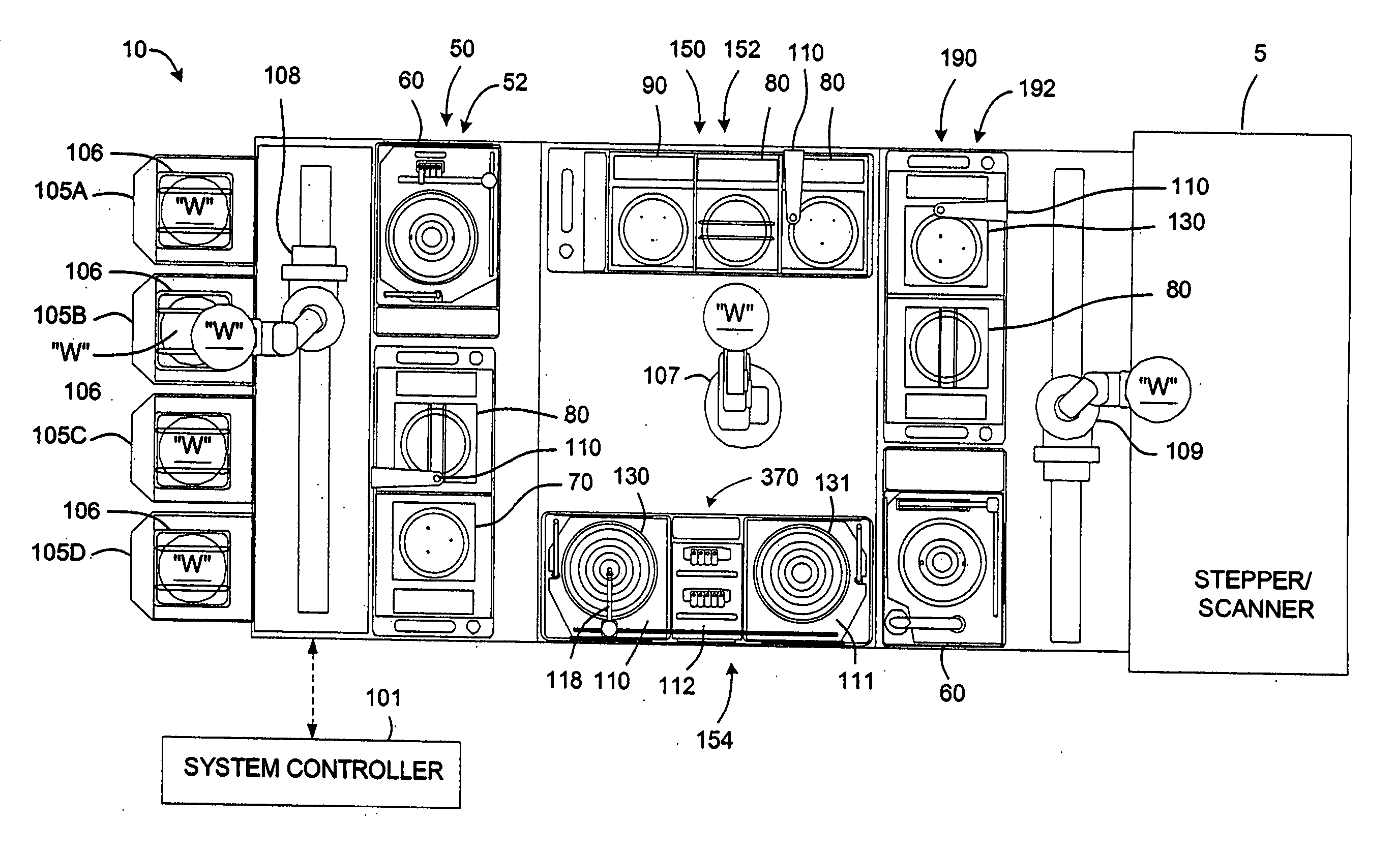
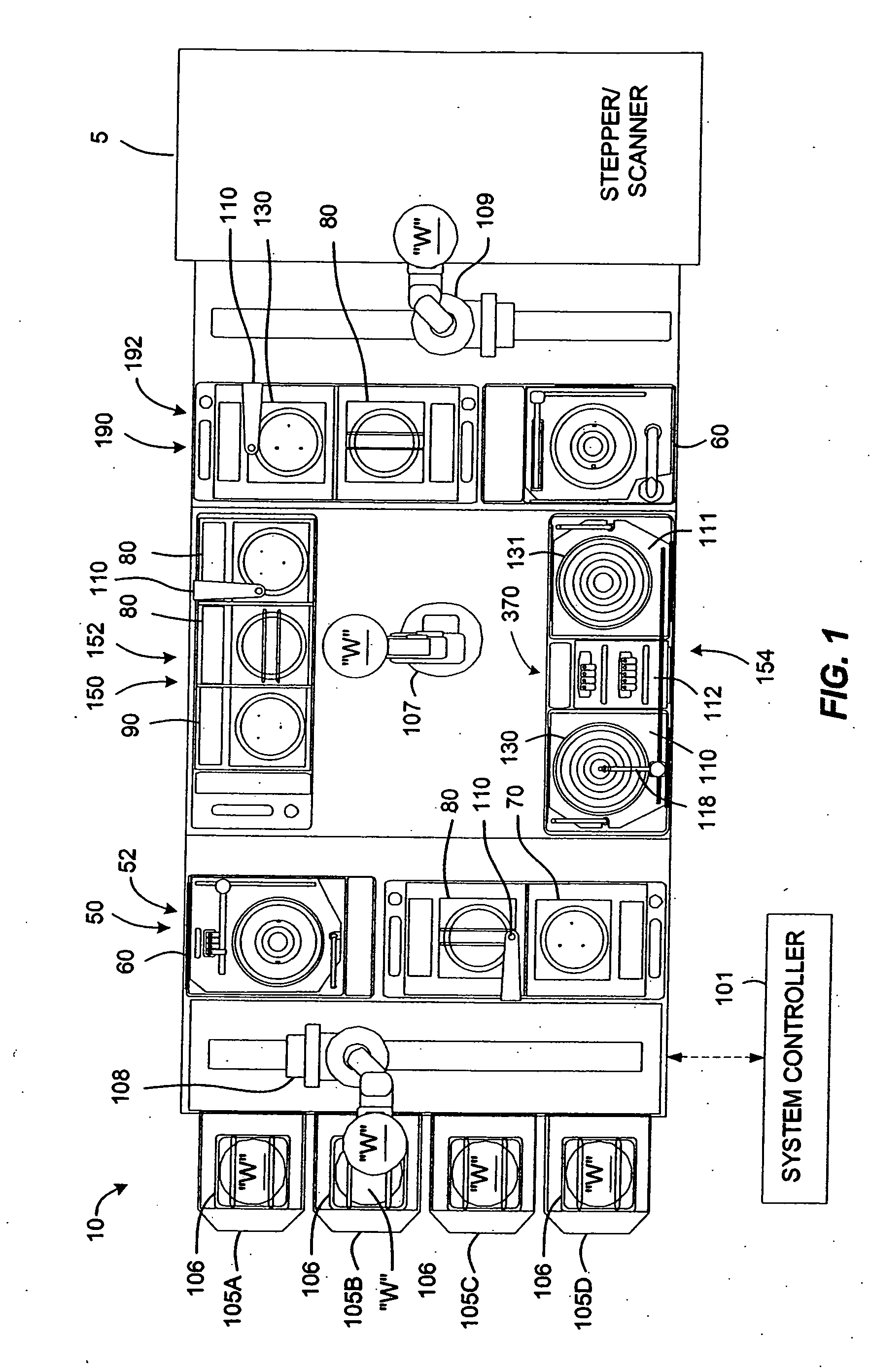
[0025]FIG. 1 is a plan view of one embodiment of a track lithography tool 10 in which the developer endpoint detection system of the present invention may be used. One embodiment of the track lithography 10, as illustrated in FIG. 1, contains a front end module (sometimes referred to as a factory interface) 50, a central module 150, and a rear module (sometimes referred to as a scanner interface) 190. The front end module 50 generally contains one or more pod assemblies or FOUPS 105 (e.g., items 105A-D), a front end ...


PUM


Abstract

A chuck for a semiconductor workpiece features integrated resistive heating and electrostatic bipolar chucking elements on a thermal pedestal. These integrated heating and chucking elements maintain wafer flatness, as well as uniformity of an underlying gap accommodating a thermal gas between the workpiece and the chuck. In accordance with one embodiment of the present invention, a laminated Kapton wafer heater is attached to the top of the thermal surface, under the wafer: At least two electrical voltage zones are isolated within the heater, in order to create a chucking force between the chuck and the wafer without having to contact the wafer with an electrical conductor. These voltage zones can be created by using separate conducting elements as well as by imposing a DC bias on zones including the resistive heating elements.

Description

CROSS-REFERENCE TO RELATED APPLICATION [0001] The instant nonprovisional patent application claims priority to U.S. provisional patent application No. 60 / 674,155, filed Apr. 21, 2005 and incorporated by reference herein for all purposes.BACKGROUND OF THE INVENTION [0002] The present invention relates generally to the field of semiconductor processing equipment. More particularly, the present invention relates to a method and apparatus for chucking and heating a semiconductor workpiece in a semiconductor processing sequence. [0003] Semiconductor device geometries have dramatically decreased in size since such devices were first introduced several decades ago. As device geometries have become more dense, reductions in the spacing between device elements has occurred. The minimum linewidths achieved using semiconductor lithography systems, sometimes referred to as a critical dimension (CD) have decreased over time. [0004] Lithography or photolithography generally refers to processes fo...

Claims


Application Information

Patent Timeline
Patent Type & Authority Applications(United States)
IPC IPC(8): H01H1/00
CPCH01L21/67103H02N13/00H01L21/6831H01L21/683B23Q3/154B23Q3/15
Inventor ISHIKAWA, TETSUYALUE, BRIAN
Owner SOKUDO CO LTD
Why Eureka
Try Eureka