Broadband optical via

a wide-band optical via and optical light guide technology, applied in the field of optical vias, can solve the problems of diffused waveguides, directional couplers, and non-use of state-of-the-art optical circuits

Active Publication Date: 2006-10-26
INFINERA CORP
View PDF10 Cites 2 Cited by
  • Summary
  • Abstract
  • Description
  • Claims
  • Application Information

AI Technical Summary

Problems solved by technology

The difficulty of directional couplers are that they are very fabrication sensitive and also naturally wavelength dependent or narrow band, and polarization dependent.
The method specifically described in U.S. Pat. No. 3,785,717 is also only limited to diffused type waveguides, which are no longer used in state of the art optical circuits.
In practice, integrated optic corner reflectors and mirrors are very difficult to fabricate and are inherently very lossy.
This loss can not be overcome easily.
Further, corner reflectors and mirrors need very high index contrast materials, or metallic layers which are inherently absorptive.
In practice these structures are very lossy, especially for single mode waveguides, and required fabrication methods that are unconventional, and therefore not suitable for mass production.
To date, such mirrors and corner reflectors have not shown promise in practice, and therefore, other means must be invented.
Further, light can not fundamentally be guided around a right-angle bend without loss and scattering.
This method uses unconventional fabrication methods and is unsuitable for volume manufacturing.
None of the prior art provides for efficient low loss power transfer between optical waveguides in a multilayer optical circuit.

Method used


Image

  • Broadband optical via
  • Broadband optical via
  • Broadband optical via

Examples


Embodiment Construction

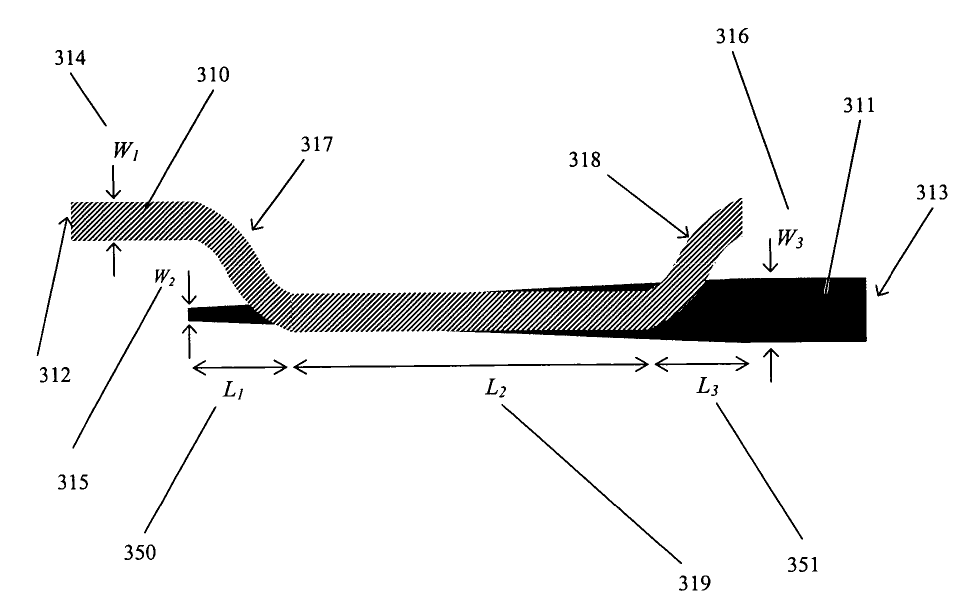
[0032] We describe here the general principle of the broadband, fabrication insensitive optical via. The via is based on the directional coupling between two waveguides situated on two vertically positioned layers, as previously described in conjunction with FIG. 2. However, in the present case the coupling strength between the two waveguides, and the relative detuning in the propagations constants, or equivalently the effective indexes, are varied as a function of propagation distance in a prescribed manner. The resulting structure is longer than the simple beat-length uniform directional coupler, but is more insensitive to exact length, wavelength, index variations, geometrical dimensions and polarization.

[0033]FIGS. 3A to 3C show schematic views of the broadband optical via invention. FIG. 3A shows a top-down schematic view of the broadband optical via. Two shaped waveguides on two different layers comprise the optical via. Waveguide 1 (310) is on planar layer 1 (347) and Wavegu...


PUM


Abstract

A broadband optical via provides a low loss interconnection between waveguides in two vertically adjacent planar waveguiding layers. Two waveguides, one in each planar layer, evanescently interact over an interaction length, and substantially all of the power on one waveguide is transferred to the second waveguide. The relative detuning between waveguides is varied along the interaction region by tapering the width of one or both guides along the direction of propagation. The interaction strength is also varied by varying the physical separation between the two waveguides such that the interaction approaches zero near the two ends of the interaction length. The performance of the broadband optical via is fabrication tolerant, polarization tolerant, wavelength tolerant, and dimensionally tolerant.

Description

CLAIM TO PRIORITY [0001] Applicants hereby claim priority under all rights to which they are entitled under 35 U.S.C. Section 119 based upon the Provisional Application Ser. No. 60 / 446,612 for this patent application filed at the United States Patent and Trademark Office on Feb. 11, 2003. CROSS-REFERENCE TO RELATED APPLICATIONS [0002] This is a continuation of application Ser. No. 10 / 776,706 Filed Feb. 11, 2004.BACKGROUND OF THE INVENTION—FIELD OF INVENTION [0003] This invention relates to a method and structure for interconnecting two integrated optical waveguides that lie in different vertical planes within a multilayer optical circuit. More specifically it relates to an optical via that transfers optical power from one waveguide to a vertically adjacent waveguide, the power transfer being fabrication tolerant, polarization tolerant, wavelength tolerant, and dimensionally tolerant. BACKGROUND OF THE INVENTION [0004] Planar optical circuits are comprised of optical waveguides and d...

Claims


Application Information

Patent Timeline
Patent Type & Authority Applications(United States)
IPC IPC(8): G02B6/26
CPCG02B6/12002G02B6/122G02B2006/12176G02B2006/12147G02B2006/12173G02B6/1228
Inventor LITTLE, BRENT E.
Owner INFINERA CORP
Why Eureka
Try Eureka