Methods and apparatus for adjusting ion implant parameters for improved process control

a technology of ion implants and parameters, applied in electrical apparatus, basic electric elements, semiconductor/solid-state device testing/measurement, etc., can solve the problems of circuit feature size decline, circuit fabrication on wafers becoming increasingly complex, and increasing the number of processing steps involved in wafer fabrication

Inactive Publication Date: 2006-10-26
VARIAN SEMICON EQUIP ASSOC INC
View PDF30 Cites 32 Cited by
  • Summary
  • Abstract
  • Description
  • Claims
  • Application Information

AI Technical Summary

Benefits of technology

[0018] In various embodiments, the implant parameter distribution may be adjusted to compensate for one or more of variation in the thickness of a polysilicon film, variation in gate polysilicon critical dimension, variation in gate sidewall offset spacer thickness, and variation in substrate crystal orientation, that result from another process step. In addition...

Problems solved by technology

Furthermore, the circuits fabricated on the wafers are becoming increasingly complex and circuit feature sizes are decreasing.
As a result of these trends, the number of processing steps involved in wafer fabrication increases, and increasingly strict requirements are placed on each of the process steps.
Further, the uniformity requirements become more stringent as integrated circuits increase in complexity.
The required degree of uniformity can be extremely difficult to achieve in many instances.
In addition, wafer parameter values in one or more process steps may fail to me...

Method used


Image

  • Methods and apparatus for adjusting ion implant parameters for improved process control
  • Methods and apparatus for adjusting ion implant parameters for improved process control
  • Methods and apparatus for adjusting ion implant parameters for improved process control

Examples


second embodiment

[0044] A simplified block diagram of an ion implantation system in accordance with the invention is shown in FIG. 4. The ion implantation system includes an ion implanter 200 and an implant controller 202. The ion implanter 200 may be any type of ion implanter. The implant controller 202 may be a general purpose computer or a special purpose controller. The ion implanter 200 and the implant controller 202 are typically integrated together to form an ion implantation system.

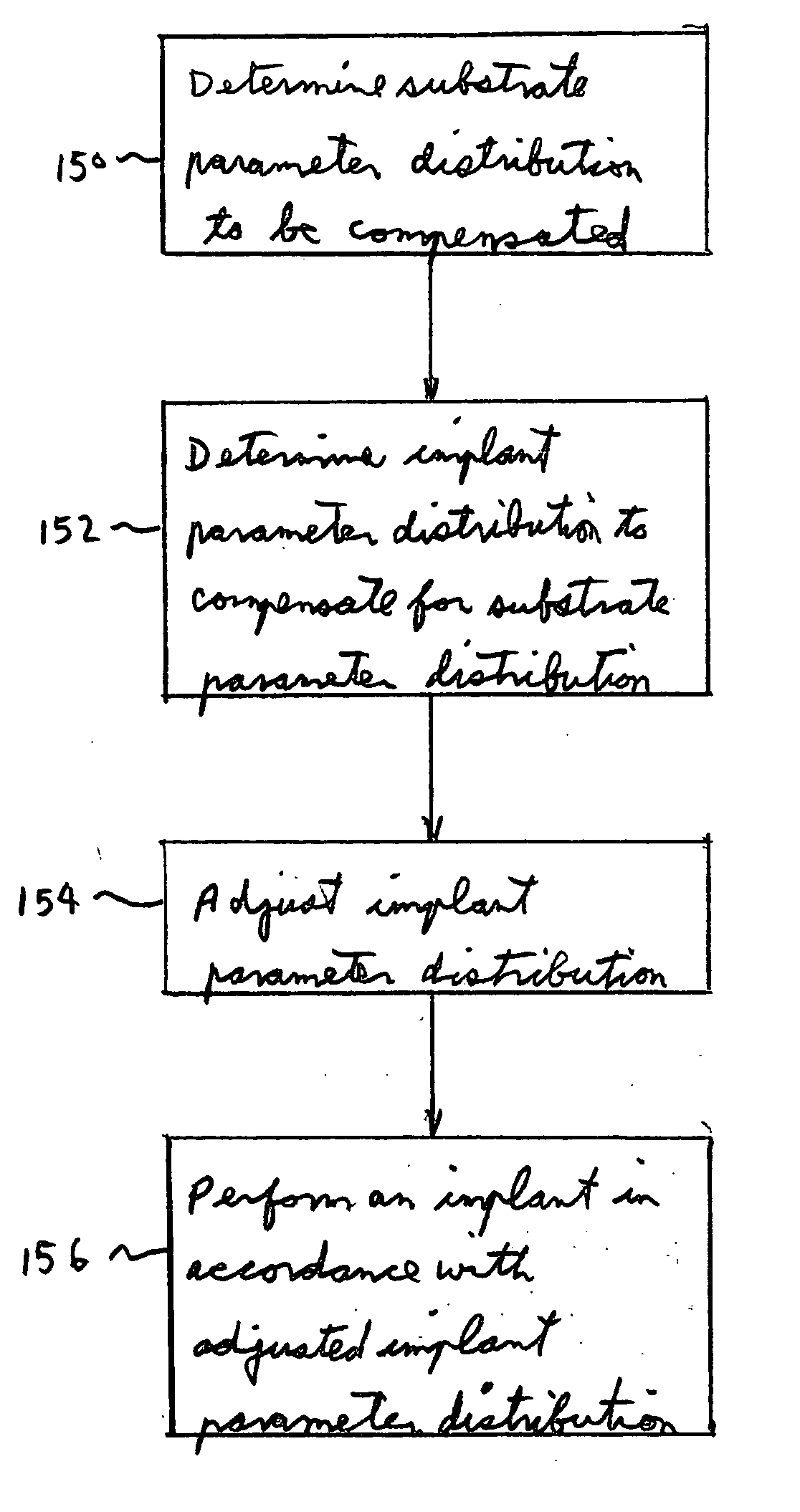
[0045] The implant controller 202 controls ion implanter 200 in accordance with an implant “recipe” for a wafer or a batch of wafers to be implanted. The recipe typically specifies parameters such as ion species, ion energy, ion dose, ion current, tilt angle, twist angle, and the like. In prior art systems, such parameters were controlled to produce a uniform implant. In accordance with aspects of the invention, a wafer parameter distribution to be compensated is input to implant controller 202. The wafer paramete...

third embodiment

[0047] A block diagram of an ion implantation system in accordance with the invention is shown in FIG. 5. The ion implantation system includes ion implanter 200 and implant controller 202. The embodiment of FIG. 5 differs from the embodiment of FIG. 4 in that the adjusted implant parameter distribution is determined off-line and is input directly to implant controller 202. Implant controller 202 uses the adjusted implant parameter distribution in conjunction with the implant recipe to control ion implanter 200. The adjusted implant parameter distribution is stored in implant controller 202 and, in effect, becomes part of the implant recipe.

[0048] The following are specific examples of process control applications in accordance with embodiments of the invention. It will be understood that these applications are given by way of example only and are not limiting as to the scope of the present invention.

[0049] Example 1 involves compensation for upstream variation in the thickness of a...


PUM


Abstract

A method for processing a substrate, such as a semiconductor wafer, includes performing a measurement to determine a substrate parameter distribution to be compensated, determining an adjusted implant parameter distribution to compensate for the substrate parameter distribution, and implanting the substrate in accordance with the adjusted implant parameter distribution. The substrate parameter distribution to be compensated may result from another process step and may be uniform or non-uniform. In another embodiment, an implant parameter may be varied as a function of implant position on the substrate to achieve different substrate parameter values in different areas of the substrate.

Description

FIELD OF THE INVENTION [0001] This invention relates to ion implantation of substrates, such as semiconductor wafers, and, more particularly, to methods and apparatus for adjusting ion implant parameters for improved process control. In some embodiments, an implant parameter distribution may be adjusted in response to a substrate parameter distribution that results from another process step and that does not meet specification. The substrate parameter distribution to be compensated may be uniform or non-uniform as a function of implant position on the substrate. In other embodiments, an implant parameter may be varied as a function of implant position on the substrate to achieve different substrate parameter values in different areas of the substrate. BACKGROUND OF THE INVENTION [0002] The processing of substrates, such as semiconductor wafers, for the manufacture of microelectronic circuits involves multiple processing steps in multiple processing tools. Such processing steps inclu...

Claims


Application Information

Patent Timeline
IPC IPC(8): H01L21/425
CPCH01L22/20
Inventor RENAU, ANTHONYRODIER, DENNISOLSON, JOSEPH C.ADAMS, BRET W.
Owner VARIAN SEMICON EQUIP ASSOC INC
Why Eureka
Try Eureka