TFT array panel, liquid crystal display including same, and method of manufacturing TFT array panel

a technology of thin film transistors and array panels, which is applied in the direction of electrical devices, semiconductor devices, instruments, etc., can solve the problems of image flickering, poor display quality, and decrease in contrast ratio, and achieve the effect of preventing light leakage curren

Inactive Publication Date: 2006-11-02
SAMSUNG DISPLAY CO LTD
View PDF5 Cites 57 Cited by
  • Summary
  • Abstract
  • Description
  • Claims
  • Application Information

AI Technical Summary

Benefits of technology

[0008] The present invention provides embodiments of a thin film transistor (TFT) array panel capable of preventing light leakage current.

Problems solved by technology

In a liquid crystal display using such a switching device, light leakage current may occur, when light is incident in a channel region of the switching device, thereby decreasing a contrast ratio or causing poor display quality such as image flickering.

Method used


Image

  • TFT array panel, liquid crystal display including same, and method of manufacturing TFT array panel
  • TFT array panel, liquid crystal display including same, and method of manufacturing TFT array panel
  • TFT array panel, liquid crystal display including same, and method of manufacturing TFT array panel

Examples


Embodiment Construction

[0022] Throughout the specification, like reference numerals refer to like elements.

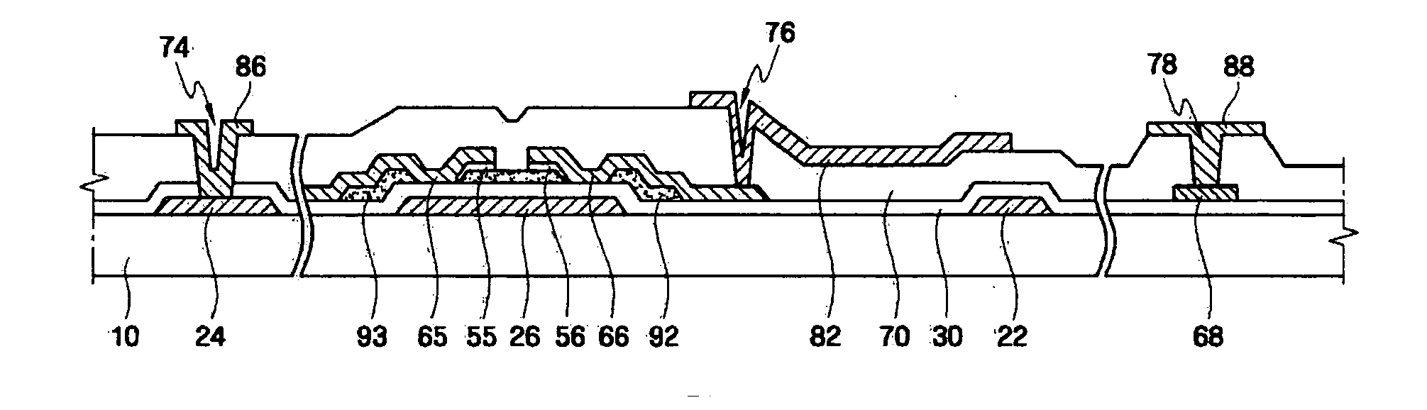
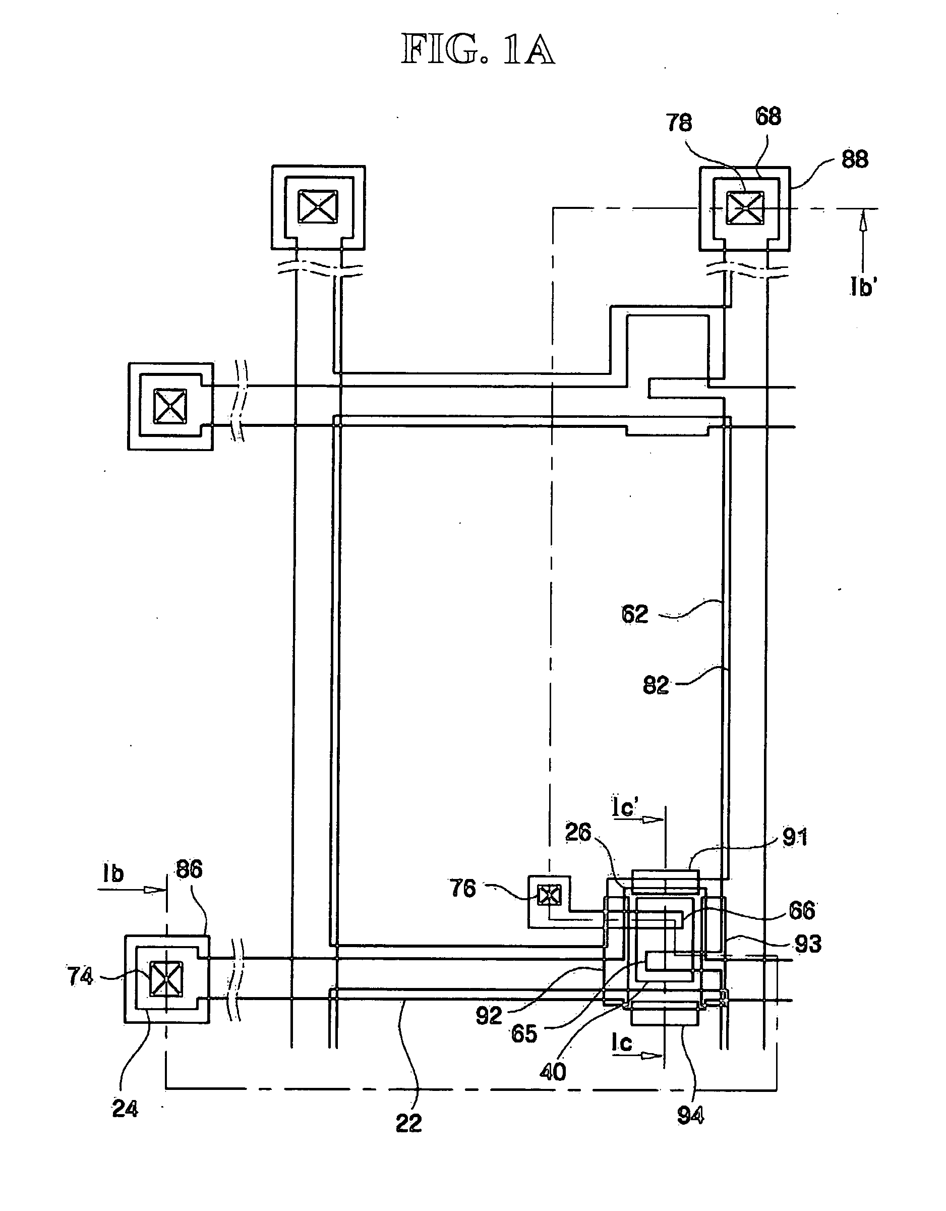
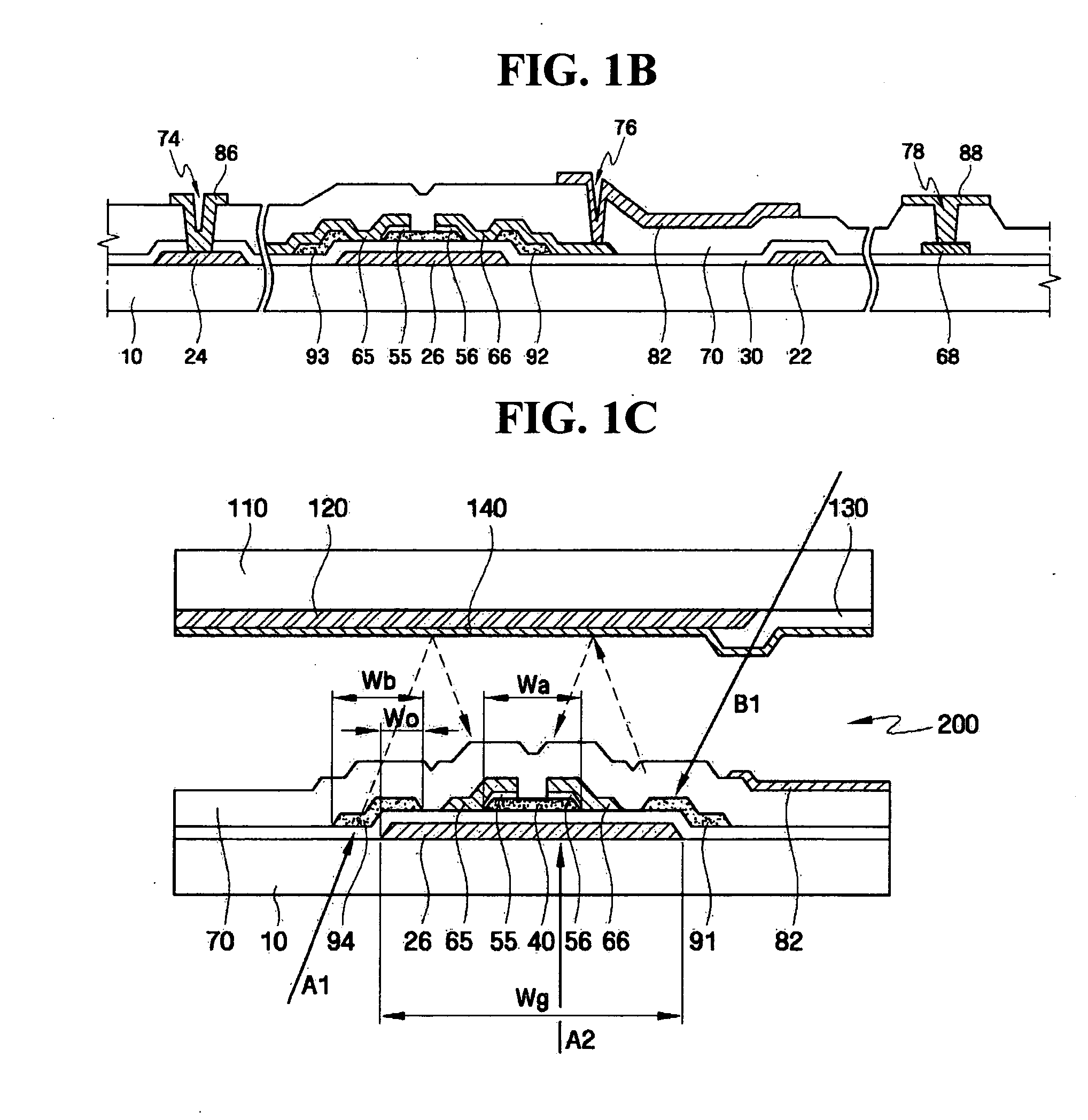
[0023] A thin film transistor (TFT) array panel for a liquid crystal display (LCD) according to an embodiment of the present invention will now be described with reference to FIGS. 1A through 1C. FIG. 1A is a circuit view of a thin film transistor (TFT) array panel according to an embodiment of the present invention, FIG. 1B is a sectional view taken along a line Ib-Ib′ of FIG. 1A, and FIG. 1C is a sectional view taken along a line Ic-Ic′ of FIG. 1A, illustrating a liquid crystal display in which a color filter panel is disposed on a TFT array panel. A TFT array panel for a liquid crystal display according to an embodiment of the present invention will first be described with reference to FIGS. 1A and 1B. Then, a liquid crystal display including the TFT array panel will be described with reference to FIG. 1C.

[0024] Referring to FIGS. 1A and 1B, gate lines 22, 24, and 26 are formed on insulating sub...


PUM

PropertyMeasurementUnit
widthaaaaaaaaaa
widthaaaaaaaaaa
dielectric constantaaaaaaaaaa

Abstract

A thin film transistor (TFT) array panel effectively minimizing light leakage current and a liquid crystal display including the same. The panel includes a transistor structure having a gate electrode formed on an insulating substrate; a semiconductor layer formed on and insulated from the gate electrode; a light blocking layer formed around and overlapping a portion of the gate electrode; a data line intersecting the gate line to form a source electrode, which overlaps a portion of the semiconductor layer; a drain electrode opposing to the source electrode and overlapping a portion of the semiconductor layer, and a pixel electrode formed on and insulated from the transistor structure and electrically connected to the drain electrode.

Description

BACKGROUND OF THE INVENTION [0001] This application claims priority from Korean Patent Application No. 10-2005-0036798, filed on May 2, 2005, in the Korean Intellectual Property Office, the disclosure of which is incorporated herein in its entirety by reference. [0002] 1. Field of the Invention [0003] The present invention relates to a thin film transistor (TFT) array panel and a liquid crystal display including the same, and a manufacturing method of the TFT array panel. More particularly, the present invention relates to a TFT array panel that can prevent the occurrence of light leakage current in a channel region, a liquid crystal display including the same, and a manufacturing method of the TFT array panel. [0004] 2. Description of the Related Art [0005] A liquid crystal display includes a color filter panel including a color filter and a thin film transistor (TFT) array panel including a TFT array. The color filter panel and the TFT array panel face with each other and are asse...

Claims


Application Information

Patent Timeline
Patent Type & Authority Applications(United States)
IPC IPC(8): H01L29/04G02F1/136
CPCG02F1/136209H01L27/12H01L29/78633G02F1/136
Inventor PARK, YONG-HANJEON, JIN
Owner SAMSUNG DISPLAY CO LTD
Why Eureka
Try Eureka