Semiconductor light-emitting device

Inactive Publication Date: 2006-11-02
SUMITOMO ELECTRIC IND LTD
View PDF5 Cites 4 Cited by
  • Summary
  • Abstract
  • Description
  • Claims
  • Application Information

AI Technical Summary

Benefits of technology

[0013] The quantum well layer may also include aluminum, gallium, indium, and arsenic, but has a composition different from that of the barrier layer. More preferably, the quantum well layer may i

Problems solved by technology

Such laser diodes are necessary to show a superior performance at high temperatures because the apparatus installing those laser diodes does not provide any temperature control means.
However, the light-emitti

Method used


Image

  • Semiconductor light-emitting device
  • Semiconductor light-emitting device
  • Semiconductor light-emitting device

Examples


Example

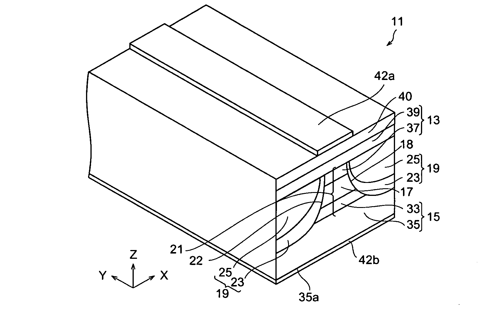
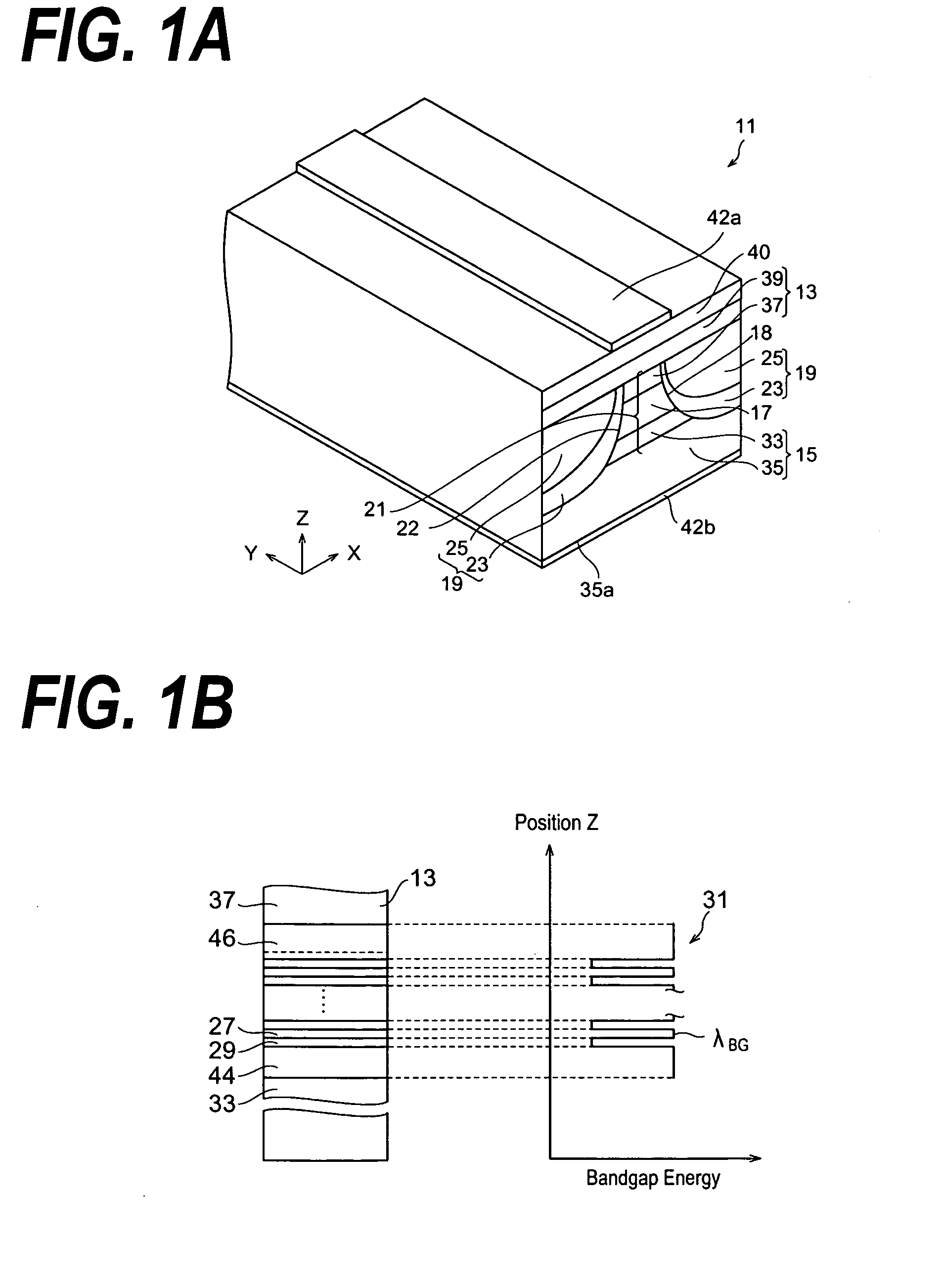
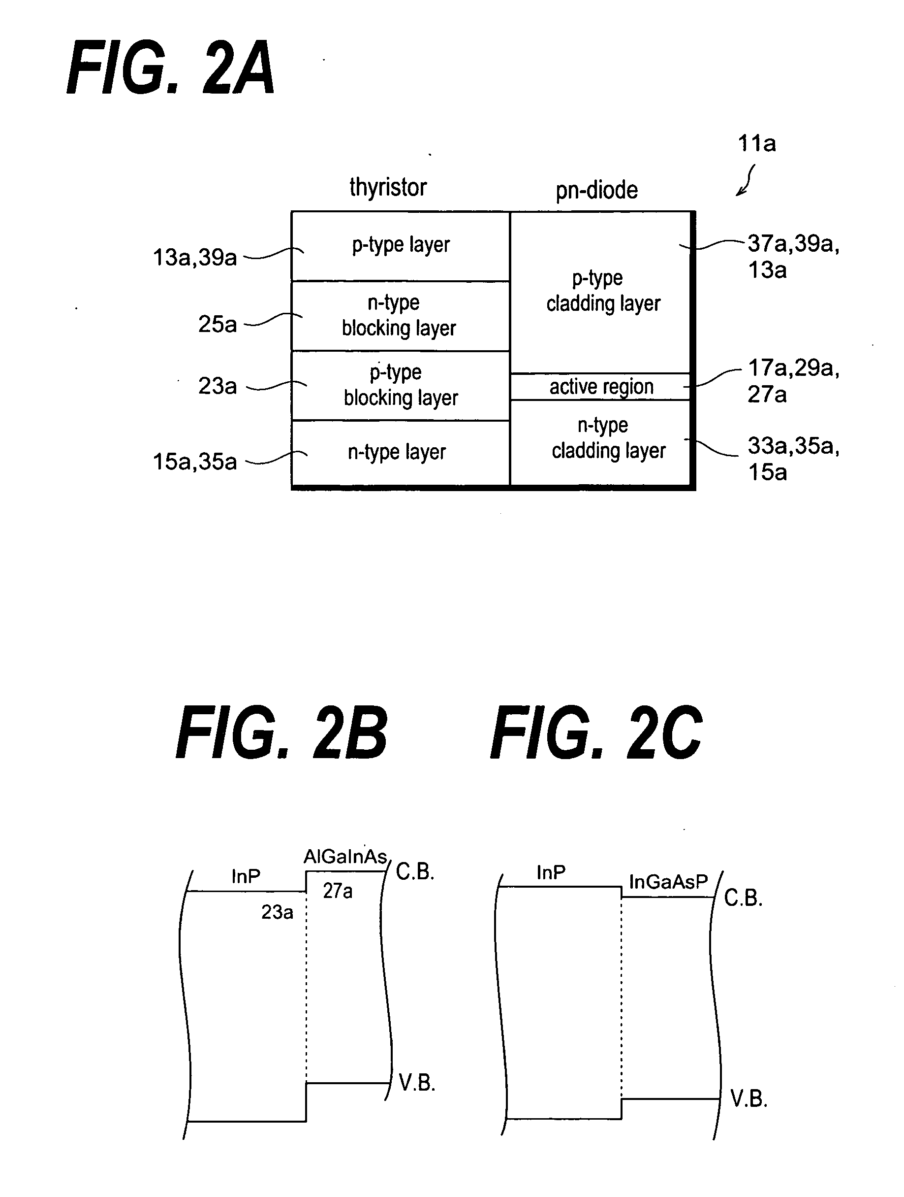
[0026]FIG. 1A shows a light-emitting device according to the first embodiment of the invention, and FIG. 1B schematically shows a structure in the active region of the light-emitting device shown in FIG. 1A. The light-emitting device 11 has a semiconductor region 13 with a second conduction type, a semiconductor region 15 with a first conduction type, an active region 17, and a buried semiconductor region 19. The active region 17 is put between the region 13 with the second conduction type and the region 33 with the first conduction type, and is within the mesa 21. The buried region 19, also put between the region 13 with the second conduction type and the region 15 with the first conduction type, and covers the side 22 of the mesa 21 and the top of the region 15 with the first conduction type. The buried region 19 includes a buried layer 23 with the second conduction type and another buried layer 25 with the firs conduction type. The former layer 23, the buried layer with the secon...

Example

Second Embodiment

[0037] The second embodiment of the present invention has a first III-V semiconductor material for the barrier layer with a tensile stress. The light-emitting device 11 according to the second embodiment, because the bottom level of the conduction band in the barrier layer may be lowered, the leak current flowing in the current blocking layer may be further reduced. Moreover, the well layer 29 may have a second III-V semiconductor material with a compressive stress to compensate the tensile stress in the barrier layer.

[0038] An example of layer configurations in the active region 17 according to the second embodiment will be shown in FIG. 11. This example is a type of the compressive stress in the well layers, while, the tensile stress in the barrier layers.

[0039] The lattice mismatching Δa / a in the well layers is greater than or equal to −1.5% and is smaller than or equal to −0.7%, where a is the lattice constant of the InP, while Δa is a difference in the latti...

Example

Third Embodiment

[0054] Next, a method for manufacturing a light-emitting device according to the present invention will be described as referring to FIGS. from 8A to 9C. In FIG. 8A, an n-type InP substrate 41 is prepared. A series of films is grown on this InP substrate 41, that is, a cladding film 43 made of an n-type InP, a lower separated-confinement-hetero-structure (SCH) film 45 made of an AlGaInAs, a multi-quantum well (MQW) region 47, an upper SCH film 49 made of an AlGaInAs, and a cladding film 51 made of a p-type InP, are grown on the InP substrate in this order. The growth of these films may be carried out in the apparatus of the Organo-Metallic Vapor-phase Epitaxy (OMVPE) technique. The MQW region 47 includes a barrier film made of the AlGaInAs with a band gap wavelength thereof greater than or equal to 1.05 μm and smaller than or equal to 1.15 μm, and a well film with a band gap wavelength longer than that of the barrier film, for example, 1.4 μm.

[0055] As shown in FIG...


PUM


Abstract

The present invention provides a light-emitting device with a quantum well structure comprising a barrier layer containing aluminum, gallium, indium and arsenic, which reduces the leak current flowing in the buried layer. The buried layer includes first and second buried layers stacked to each other and covers the sides of the quantum well structure. The barrier layer induces a tensile stress to lower the band gap energy, to increase the band gap wavelength λBG greater than or equal to 1.0 μm.

Description

RELATED APPLICATIONS [0001] This application is a continuation-in-part application of application Ser. No. 11 / 020,662, filed Dec. 27, 2004, entitled “Semiconductor light-emitting device,” and assigned to the Assignee of the present application. This application is closely related to a pending application, Ser. No. of which is 11 / 280,823, filed Nov. 17, 2005, entitled “Distributed feedback laser including AlGaInAs in feedback grating layer.”BACKGROUND OF THE INVENTION [0002] 1. Field of the Invention [0003] The present invention relates to a semiconductor light-emitting device, in particular, relates to a semiconductor laser diode. [0004] 2. Related Prior Art [0005] As increasing a mass of the optical communication, light-emitting devices able to be modulated with higher frequencies and to be produced with lower cost are required. Semiconductor laser diodes with emitting wavelengths within 1.3 μm band by directly modulating without any control means of temperatures there of such as a...

Claims


Application Information

Patent Timeline
IPC IPC(8): H01L33/00
CPCB82Y20/00H01S5/2222H01S5/227H01S5/34366H01S5/3403H01S5/34306H01S5/2275
Inventor IKOMA, NOBUYUKIKAWAHARA, TAKAHIKOFURUKAWA, MASATO
Owner SUMITOMO ELECTRIC IND LTD
Why Eureka
Try Eureka