Eureka AIR delivers breakthrough ideas for toughest innovation challenges, trusted by R&D personnel around the world.

Random number generation circuit

Inactive Publication Date: 2006-11-02
KK TOSHIBA
View PDF4 Cites 22 Cited by
  • Summary
  • Abstract
  • Description
  • Claims
  • Application Information

AI Technical Summary

Benefits of technology

[0014] a serial-parallel converter which generates random parallel data used for controlling a dela

Problems solved by technology

However, it is not possible to reduce the probability of collision of finally obtained random numbers unless the seed to be input to the feedback shift register has a sufficient level of randomness.
The probability of collision of random numbers depends on the uncertainty of the seed generated by the flip-flop and this uncertainty mainly depends on the fact that the oscillation circuit composed of the CMOS inverters is unstable with respect to fluctuation of temperature and supply voltage.
Therefore, it is difficult for the conventional method to reduce the probability of collision of random numbers.
In this way, the conventional random number generation circuit has a problem that it is not possible to obtain high quality random numbers.

Method used


Image

  • Random number generation circuit
  • Random number generation circuit
  • Random number generation circuit

Examples


first embodiment

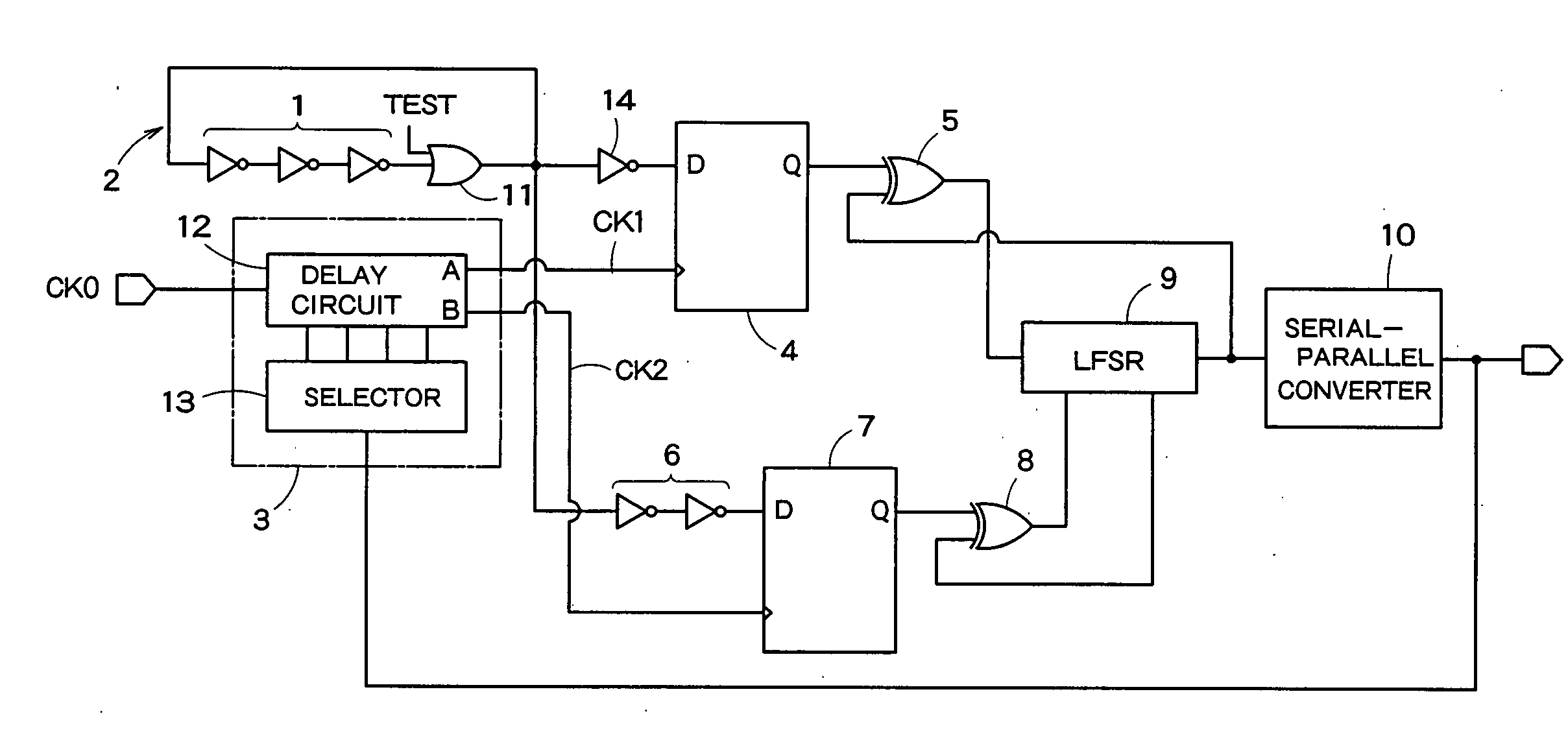
[0038]FIG. 1 is a block diagram showing a schematic configuration of a random number generation circuit according to an embodiment of the present invention. The random number generation circuit in FIG. 1 is provided with a ring oscillator 2 which has an odd number of cascaded inverters 1, a delay control circuit 3 which delays a reference clock signal CK0 to generate delay reference clock signals CK1, CK2, a first flip-flop 4 which latches the oscillation signal generated by the ring oscillator 2 with the delay reference clock signal CK1, a first EXOR circuit 5 which equalizes occurrence frequency with which output logics “0”, “1” of the first flip-flop 4 appear, a delay circuit 6 which delays the oscillation signal generated by the ring oscillator 2, a second flip-flop 7 which latches the oscillation signal delayed by the delay circuit 6 with the delay reference clock signal CK2, a second EXOR circuit 8 which equalizes occurrence frequency with which output logics “0”, “1” of the s...

second embodiment

[0074] A second embodiment is designed to randomize phase fluctuations of an oscillation signal generated by a ring oscillator.

[0075]FIG. 6 is a block diagram showing a schematic configuration of a random number generation circuit according to a second embodiment of the present invention. In FIG. 6, components common to those in FIG. 1 are assigned the same reference numerals and the following explanations will be focused on the differences.

[0076] The random number generation circuit in FIG. 6 is provided with a ring oscillator 2a having an internal configuration different from that in FIG. 1, a first flip-flop 4 which latches the output signal of the ring oscillator 2a, a first ExOR circuit 5 which equalizes occurrence frequency with which output logics “0”, “1” of the first flip-flop 4 appear, a linear feedback register 9 (LFSR) which generates random numbers (random serial data) based on the output signal of the first ExOR circuit 5 and a serial-parallel converter 10 which conv...

third embodiment

[0105] A third embodiment is a modification example of the second embodiment and provides a ring oscillation type VCO instead of the ring oscillator 2a.

[0106]FIG. 10 is a circuit diagram showing internal configuration of a ring oscillation type VCO 2b used in the third embodiment. This ring oscillation type VCO 2b is used in place of the ring oscillator 2a in FIG. 6 and the rest of components within the random number generation circuit are the same as those in FIG. 6, and therefore those components are omitted in FIG. 10.

[0107] The ring oscillation type VCO 2b in FIG. 10 is provided with an odd number of inverting amplifiers 61 connected in a ring shape and an odd number of voltage control circuits 69 which perform voltage control of the respective drive capabilities of the odd number of inverting amplifiers 61.

[0108] Each inverting amplifier 61 in the ring oscillation VCO 2b includes a PMOS transistor 64 and NMOS transistor 65. The voltage control circuit 69 provided for each in...


PUM


Abstract

A random number generation circuit has a ring oscillator which has odd number of inverting amplifiers connected in ring shape, a delay control circuit which generates a predetermined clock signal by delaying a reference clock signal, a first sampling circuit which samples an oscillation signal generated by the ring oscillator with the predetermined clock signal, a first logical equalization circuit which equalizes occurrence frequency of “0” and “1” of a sampling signal sampled by the first sampling circuit, a linear feedback shift register (LFSR) which generates random serial data based on an output signal of the first logical equalization circuit, and a serial-parallel converter which generates random parallel data used for controlling a delay amount of the delay control circuit by converting the random serial data from serial to parallel.

Description

CROSS REFERENCE TO RELATED APPLICATIONS [0001] This application is based upon and claims the benefit of priority from the prior Japanese Patent Applications No. 2005-73444, filed on Mar. 15, 2005 and No. 2006-67462, filed on Mar. 13, 2006, the entire contents of which are incorporated herein by reference. BACKGROUND OF THE INVENTION [0002] 1. Field of the Invention [0003] The present invention relates to a random number generation circuit which generates random numbers. [0004] 2. Related Art [0005] A random number generation circuit provided with an oscillation circuit connected to one or three CMOS inverters, a flip-flop which latches an oscillation signal generated by this oscillation circuit and a feedback shift register which generates pseudo-random numbers based on an output signal of the flip-flop is known (see Japanese Patent Laid-Open No. 2002-236582). [0006] This type of conventional random number generation circuit inputs the output signal of the flip-flop as a seed to the...

Claims


Application Information

Patent Timeline
IPC IPC(8): H03K3/03
CPCH03K3/0315G06F7/588H03K3/84H03K3/354
Inventor SUZUKI, TAKETOSHI
Owner KK TOSHIBA
Why Eureka
Eureka Blog
Learn More