Mitigation of RF Oscillator Pulling through Adjustable Phase Shifting

a phase shifting and oscillator technology, applied in the field of radio frequency transmitters and data communications, can solve the problems of modulation distortion, inability to cost effectively add features and reduce footprint, and inability to meet the design challenges of advanced processes,

Inactive Publication Date: 2010-11-11
TEXAS INSTR INC
View PDF2 Cites 43 Cited by
  • Summary
  • Abstract
  • Description
  • Claims
  • Application Information

AI Technical Summary

Problems solved by technology

However, for analog / RF designs, the immaturity of advanced processes comes with design challenges that may outweigh the intended advantage.
In older generation handsets, 30% to 40% of handset board space is occupied by analog / RF functionality which cannot be re-designed or migrated to the newer process / technology nodes easily, inhibiting vendor ability to cost effectively add features and reduce footprint.
EDGE transmitters, as well as other non-constant amplitude transmitters, may be affected by modulation distortion due to the RF oscillator pulling by the transmitted RF output and supply-ground coupling of extraneous noise sources.
For example, the aggressing signal may cause capacitance changes in the resonance circuit that correspond to the amplitude fluctuations in it, thereby creating parasitic frequency modulation.
Additionally, supply-ground coupling of current generated by the transmitter's amplitude modulation circuitry integrated on the same die causes frequency pushing of the oscillator.
In a typical EDGE transmitter, amplitude modulation in the pre-power amplifier (PPA) causes frequency pulling of the DCO, thus leading to performance degradation in both error-vector-magnitude (EVM) and modulation spectrum.
Both of these methods significantly increase the hardware complexity and the power consumption.
Unlike most of the RF-friendly processes, CMOS does not offer significant DC resistance between two circuits, i.e., the RF oscillator and the PPA or PA, the transistors of which are tied to the same substrate through the back gate.

Method used


Image

  • Mitigation of RF Oscillator Pulling through Adjustable Phase Shifting
  • Mitigation of RF Oscillator Pulling through Adjustable Phase Shifting
  • Mitigation of RF Oscillator Pulling through Adjustable Phase Shifting

Examples


Embodiment Construction

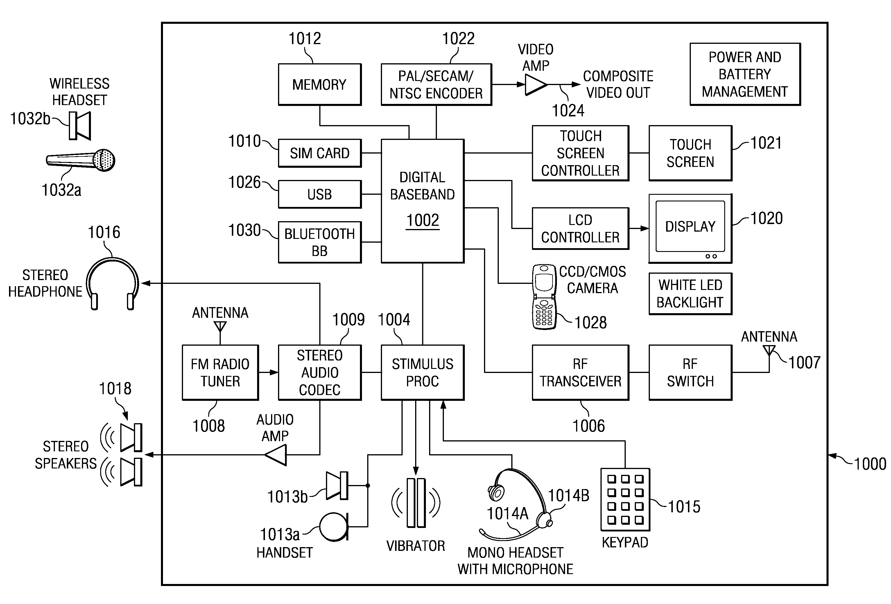
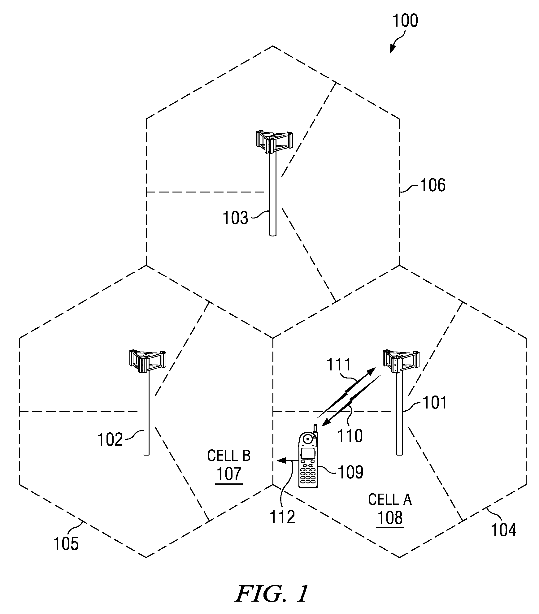
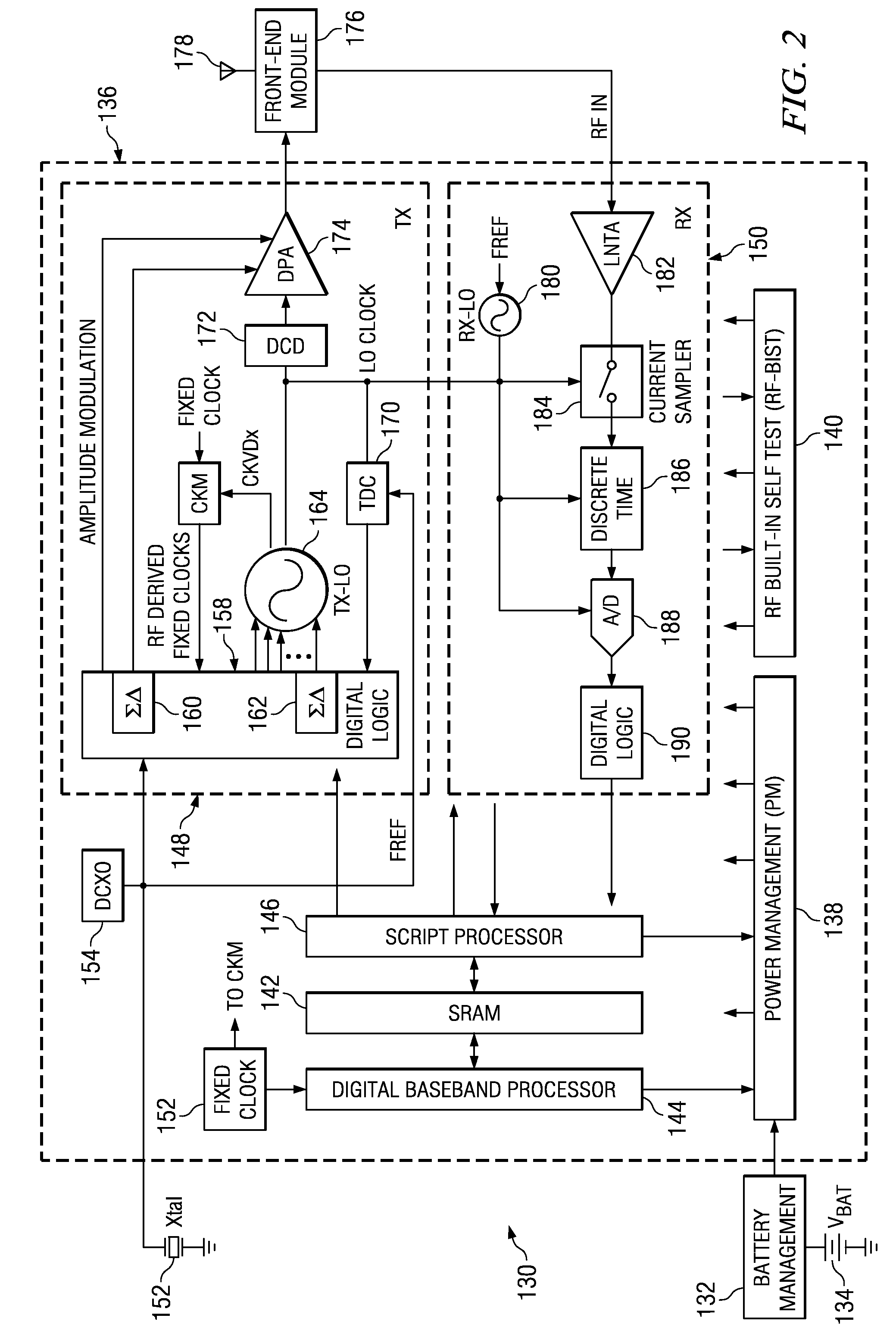
[0025]Embodiments of the present invention provide for mitigation of frequency-pulling of a digitally controlled oscillator (DCO) due to pre-power amplifier (PPA) activity. An adjustable phase delay is provided between the DCO and the PPA. In one embodiment, the adjustable phase delay is provided through a chain of inverters. The delay may be calibrated using a phase error (PHE) signal from a phase detector in a phase locked loop (PLL) that forms the DCO. The PHE reflects the extent of parasitic modulation suffered by the DCO as a result of pulling; hence the variance of this signal, as well as other properties of it extracted through appropriate processing, can be used to sense the extent of pulling and calibrate for optimum delay. In one embodiment, this delay is calibrated in the center of the Digital Cellular System (DCS1800) and Personal Cellular System (PCS1900) bands. Frequency-dependent fine-tuning of the delay, referred to as frequency compensation, can be based on the comp...


PUM


Abstract

A digitally controlled mechanism for the minimization of the self-interference caused by an amplitude modulated signal generated within a polar transmitter to the oscillator circuit, where the carrier of that transmitter is created. A digitally controlled delay between the circuit where the signal is generated and the circuit where it is amplitude-modulated allows adjustment of the delay or phase-shift between the aggressing and victim signals. The optimal delay that is to be introduced in the path is determined, and a corresponding control word is generated to arrive at the selected delay / phase-shift.

Description

FIELD OF THE INVENTION[0001]This invention generally relates to the field of radio frequency transmitters and data communications. In particular, it relates to cellular telephony and communication devices such as Bluetooth, WLAN, and cellular transceivers using digitally-intensive radio frequency (RF) circuitry.BACKGROUND OF THE INVENTION[0002]Wireless cellular communication networks incorporate large numbers of mobile user equipment (UEs) and a number of base nodes (NodeBs). A NodeB is generally a fixed station, and may also be called a base transceiver system (BTS), an access point (AP), a base station (BS), or some other equivalent terminology. As improvements of networks are made, the NodeB functionality evolves, so a NodeB is sometimes also referred to as an evolved NodeB (eNB). In general, NodeB hardware, when deployed, is fixed and stationary, while the UE hardware is typically portable. In contrast to NodeB, the mobile UE can comprise portable hardware.[0003]User equipment (...

Claims


Application Information

Patent Timeline
Patent Type & Authority Applications(United States)
IPC IPC(8): G01S7/40H04M1/00
CPCH04B15/02H04B1/0475
Inventor BASHIR, IMRANSTASZEWSKI, ROBERT BOGDANELIEZER, ORENLEE, MENG-CHANG
Owner TEXAS INSTR INC
Why Eureka
Try Eureka