

Wiring board, multilayer wiring board, and method for manufacturing the same
a wiring board and multi-layer technology, applied in the manufacture of printed circuits, printed circuit aspects, basic electric elements, etc., can solve the problems of reducing size and thickness, reducing difficulty in mounting electronic components, so as to improve the degree of flexibility in design, increase the mounting density of components on the conductive layer surface, and the effect of compactness
- Summary
- Abstract
- Description
- Claims
- Application Information
AI Technical Summary
Benefits of technology
Problems solved by technology
Method used
Image

Examples
first embodiment
[0129] The manufacturing method of this embodiment differs from manufacturing method of the first embodiment in that, after first stacking onto the wiring board 10 an outer-layer wiring substrate 13 on which a wiring pattern has not yet been formed, the wiring pattern is formed in the outer layer-side conductive layer 6. The following is a detailed explanation.
[0130] As shown in FIG. 14 and FIG. 15, outer-layer wiring substrates 13 in the outer layer-side conductive layers 6 of which a wiring pattern has not been formed are stacked onto both surfaces of a wiring board 10, and by performing pressing in the thickness direction, the outer-layer wiring substrates 13 and wiring board 10 are bonded together.
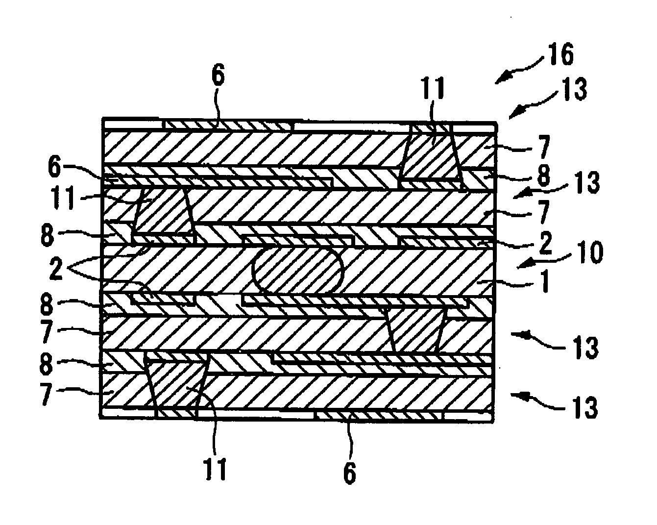
[0131] Next, as shown in FIG. 16, a pattern of wiring is formed in the outer layer-side conductive layers 6 of the outer-layer wiring substrates 13, to obtain the multilayer wiring board 15.
[0132] As shown in FIG. 17 and FIG. 18, additional layers may be added to the multilayer wirin...
second embodiment
[0134] According to the manufacturing method of the above second embodiment since a wiring pattern is formed in the outer layer-side conductive layers 6 after stacking outer-layer wiring substrates 13 onto a wiring board 10, adverse effects of the pressing process on wiring may be prevented. Hence, the wiring of the outer layer-side conductive layers 6 may be made even finer.
[0135] Next a third nonlimiting exemplary embodiment of a method for manufacturing a multilayer wiring board of the present invention is explained.
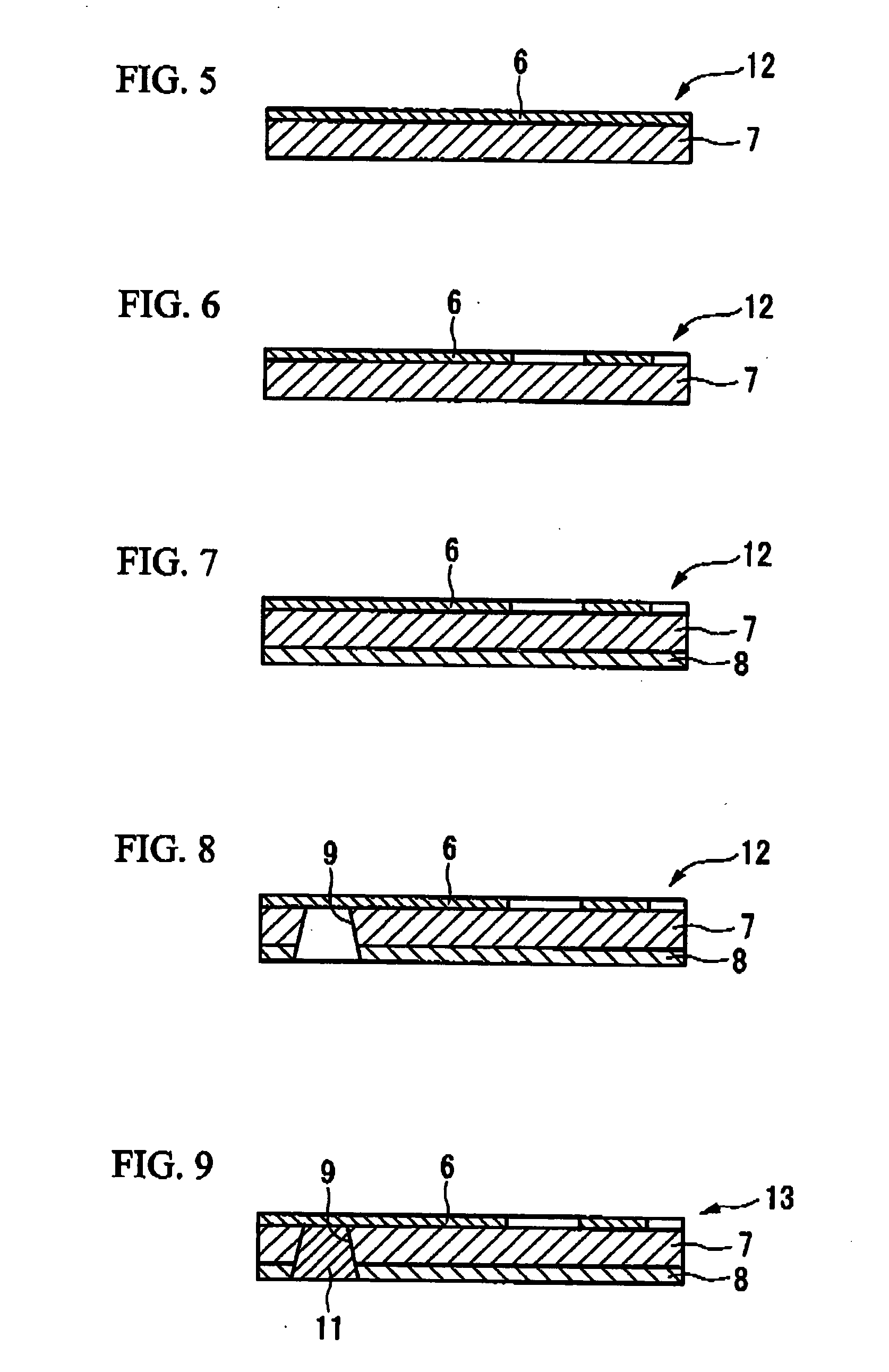
[0136] The manufacturing method of this embodiment differs from the manufacturing method of the fist embodiment in that, after first stacking onto the wiring board 10 an outer-layer wiring substrate 13a in which an opening 9 and connecting portion 11 have not yet been formed, the opening 9 and connecting portion 11 are formed. The following is a detailed explanation.
[0137] As shown in FIG. 19, outer-layer wiring substrates 13a in which an opening 9 and connecting po...
third embodiment
[0141] According to the method of manufacturing of the above third embodiment, after stacking outer-layer wiring substrates 13a to a wiring board 10, the openings 9 and connecting portions 11 are formed, so that the connecting portions may be reliably brought into contact with the conducting layers 2 and 6, and the conductivity therebetween may be improved. Hence, the reliability of electrical connections may be improved.
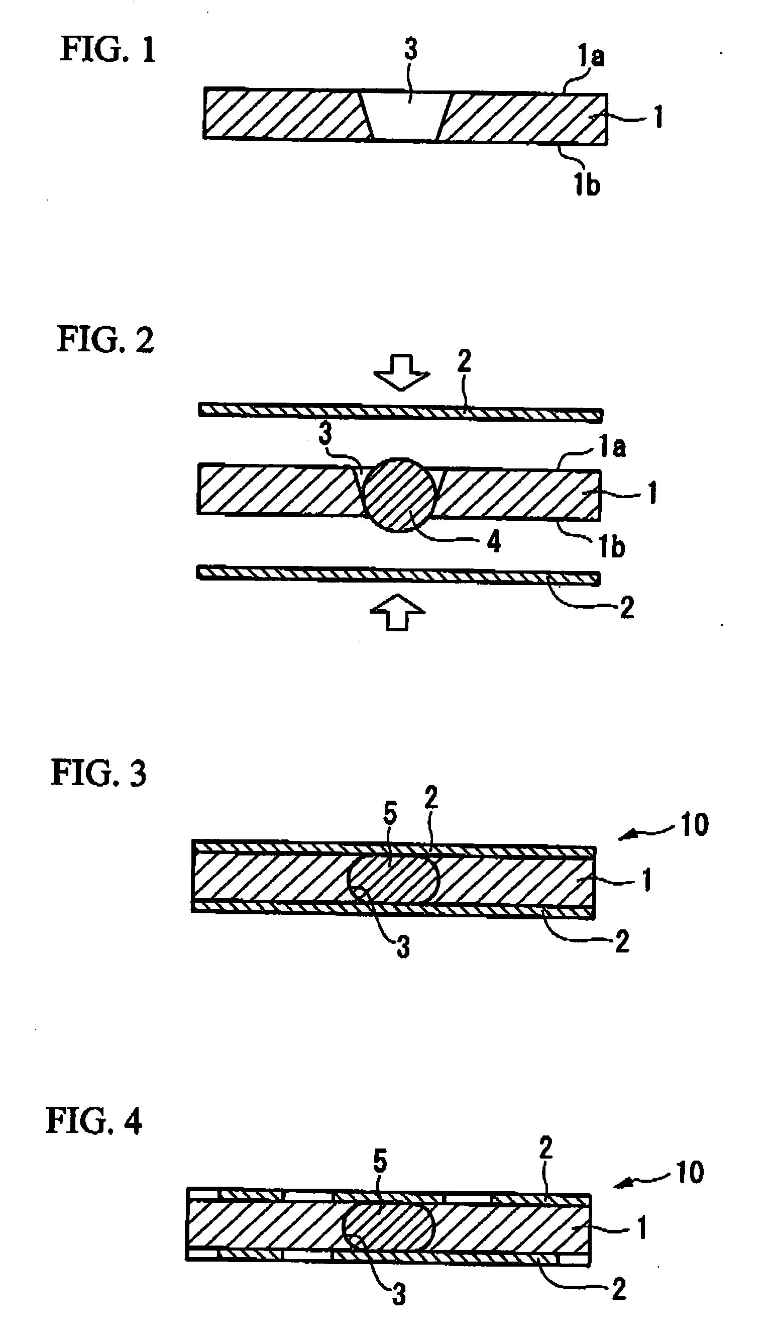
[0142] According to the manufacturing methods of the first through third embodiments, as shown in FIG. 1 through FIG. 4, when manufacturing the wiring board 10, the connecting particle 4 is placed into the penetrating hole 3, and by performing pressing in the thickness direction, the particle is deformed into the connecting member 5. However, the wiring board 10 may also be manufactured by the method described below.
[0143] As shown in FIG. 24, printing or other means are used to provide a protrusion for connection 18 on one surface (the lower surface) of an inner l...
PUM
| Property | Measurement | Unit |
|---|---|---|
| Thickness | aaaaa | aaaaa |
| Diameter | aaaaa | aaaaa |
| Electrical conductor | aaaaa | aaaaa |
Abstract
Description
Claims
Application Information