

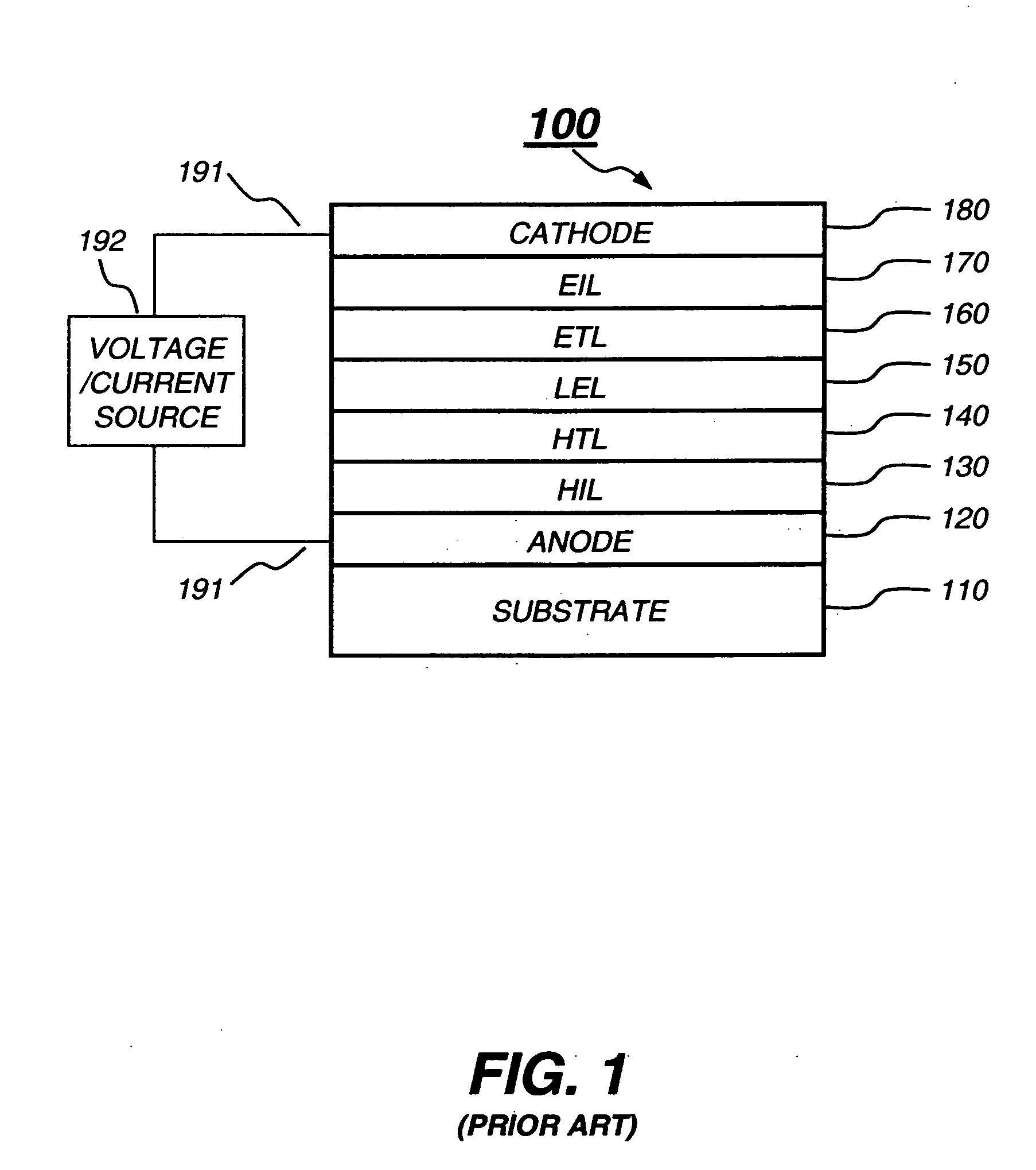
OLED electron-injecting layer
a technology of electron injection and oled, which is applied in the direction of discharge tube luminescnet screen, other domestic articles, natural mineral layered products, etc., can solve the problems of insufficient electron recombination in lel, unbalanced electron-hole recombination, and difficult or impossible electron injection from the etl into the lel
- Summary
- Abstract
- Description
- Claims
- Application Information
AI Technical Summary
Benefits of technology
Problems solved by technology
Method used
Image

Examples
example 6 (
Inventive)
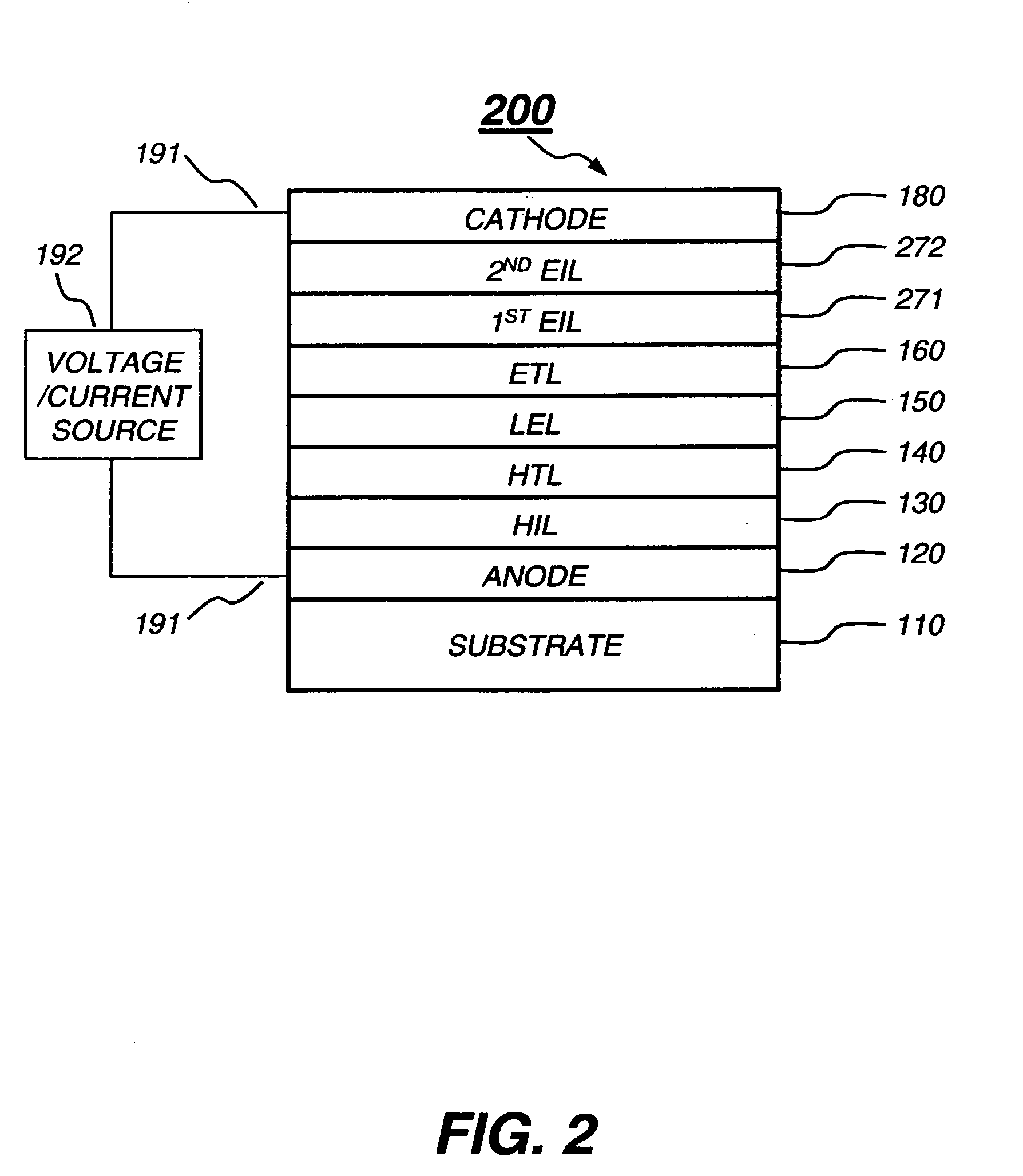
[0141] An OLED in accordance with the present invention was constructed as the same as that in Example 4, except that the layer c in Example 4 was replaced by:
[0142] c) the 1st EIL, 29 nm thick, composed of Alq doped with about 1.2 vol % lithium; and
[0143] d) the 2nd EIL, 1 nm thick, composed of HAT-CN.
[0144] This OLED, having the 2nd EIL in direct contact with the 1st EIL, requires a drive voltage of about 5.0 V to pass 20 mA / cm2. Under this test condition, the device has a luminance of 1891 cd / m2, and a luminous efficiency of about 9.5 cd / A. Its emission peak is at 521 nm. The operational lifetime, measured as T50(RT@80 mA / cm2), is about 312 hours. The average rate of the voltage rise during the lifetime testing is about 3.5 mV / hr. Its normalized luminance vs. operational time and its drive voltage vs. operational time, tested at room temperature and at 80 mA / cm2, are shown in FIGS. 6 and 7, respectively.
[0145]FIGS. 6 and 7 demonstrate that the OLED constructed in ac...
example 7 (
Inventive)
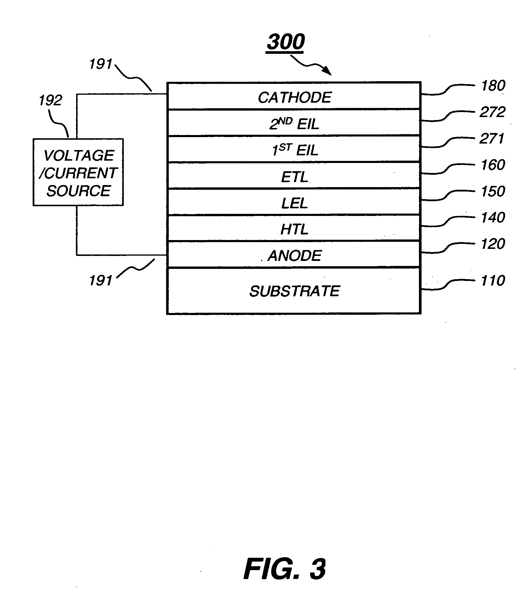
[0146] Another OLED in accordance with the present invention was constructed in the same general manner as that in Example 1. But, the layer structure of the EL unit is as follows:
[0147] a) an HIL, 10 nm thick, composed of HAT-CN;
[0148] b) an HTL, 65 nm thick, composed of NPB;
[0149] c) a LEL, 30 nm thick, composed of Alq doped with 1.0 vol % C545T;
[0150] d) the 1st EIL, 20 nm thick, composed of Alq doped with about 1.2 vol % lithium; and
[0151] e) the 2nd EIL, 10 nm thick, composed of HAT-CN.
[0152] This OLED requires a drive voltage of about 5.1 V to pass 20 mA / cm2. Under this test condition, the device has a luminance of 1823 cd / m2, and a luminous efficiency of about 9.1 cd / A. Its emission peak is at 521 nm. The operational lifetime, measured as T50(RT@80 mA / cm2), is about 350 hours. The average rate of the voltage rise during the lifetime testing is about 2.9 mV / hr. Its normalized luminance vs. operational time and its drive voltage vs. operational time, tested at r...
example 8 (
Inventive)
[0153] Another OLED was constructed in accordance with the present invention. This OLED is the same as that in Example 7, except that layers d and e were changed as follows:
[0154] d) the 1st EIL, 5 nm thick, composed of Alq doped with about 1.2 vol % lithium; and
[0155] e) the 2nd EIL, 25 nm thick, composed of HAT-CN doped with about 1.2 vol % lithium.
[0156] This OLED requires a drive voltage of about 4.6 V to pass 20 mA / cm2. Under this test condition, the device has a luminance of 1898 cd / m2, and a luminous efficiency of about 9.5 cd / A. Its emission peak is at 521 nm. The operational lifetime, measured as T50(RT@80 mA / cm2), is about 330 hours. The average rate of the voltage rise during the lifetime testing is about 2.1 mV / hr. Its normalized luminance vs. operational time and its drive voltage vs. operational time, tested at room temperature and at 80 mA / cm2, are shown in FIGS. 8 and 9, respectively.
[0157] It is evident from FIGS. 8 and 9 that the OLEDs having a Li-dop...
PUM
| Property | Measurement | Unit |
|---|---|---|
| reduction potential | aaaaa | aaaaa |
| reduction potential | aaaaa | aaaaa |
| optical band gap | aaaaa | aaaaa |
Abstract
Description
Claims
Application Information