
Substrate conveyance device and substrate conveyance method, exposure apparatus and exposure method, device manufacturing method

a technology of substrate conveyance and conveyance device, which is applied in the direction of photosensitive materials, instruments, printers, etc., can solve the problems of reducing device productivity and insufficient focus margin during exposure operation, and achieve the effect of high device productivity

Inactive Publication Date: 2006-11-16
ZAO NIKON +1
View PDF46 Cites 46 Cited by
  • Summary
  • Abstract
  • Description
  • Claims
  • Application Information

AI Technical Summary

Benefits of technology

[0013] According to the present invention, the liquid adhering on the substrate can be detected when the substrate experienced the liquid immersion exposure is conveyed. Further, based on the detection results, in the case, for example, where the liquid is adhering on the substrate, the substrate can be, after removing the liquid therefrom, sent to a post-exposure process, e.g., a development process. Thus, a device having a desired performance can be produced without being affected by the liquid in the post-exposure process. Further, when it is detected that the liquid is not adhering on the substrate, the liquid removal process can be omitted, which improves the operation efficiency. In addition, by executing again the liquid detection process on the substrate after the liquid removal process, it can be detected whether the liquid removal has been performed well. In this way, based on the detection results from the liquid detector, appropriate steps to maintain high device productivity can be taken.
[0017] In accordance with the present invention, based on the detection results from the liquid detector, appropriate steps to maintain high device productivity can be taken, and thus a device having a desired performance can be produced.

Problems solved by technology

When the depth of focus 6 becomes too narrow, it becomes difficult to make the substrate surface coincide with the image plane of the projection optical system, and thus there occurs the possibility that the focus margin during the exposure operation will be insufficient.
As just described, when the liquid remaining on a substrate having been liquid immersion exposed is left as it is, a device defect is induced; however, such a defect is found as a form of a defective product only after completing a final device, which may cause decrease of device productivity.

Method used


Image

  • Substrate conveyance device and substrate conveyance method, exposure apparatus and exposure method, device manufacturing method
  • Substrate conveyance device and substrate conveyance method, exposure apparatus and exposure method, device manufacturing method
  • Substrate conveyance device and substrate conveyance method, exposure apparatus and exposure method, device manufacturing method

Examples


Embodiment Construction

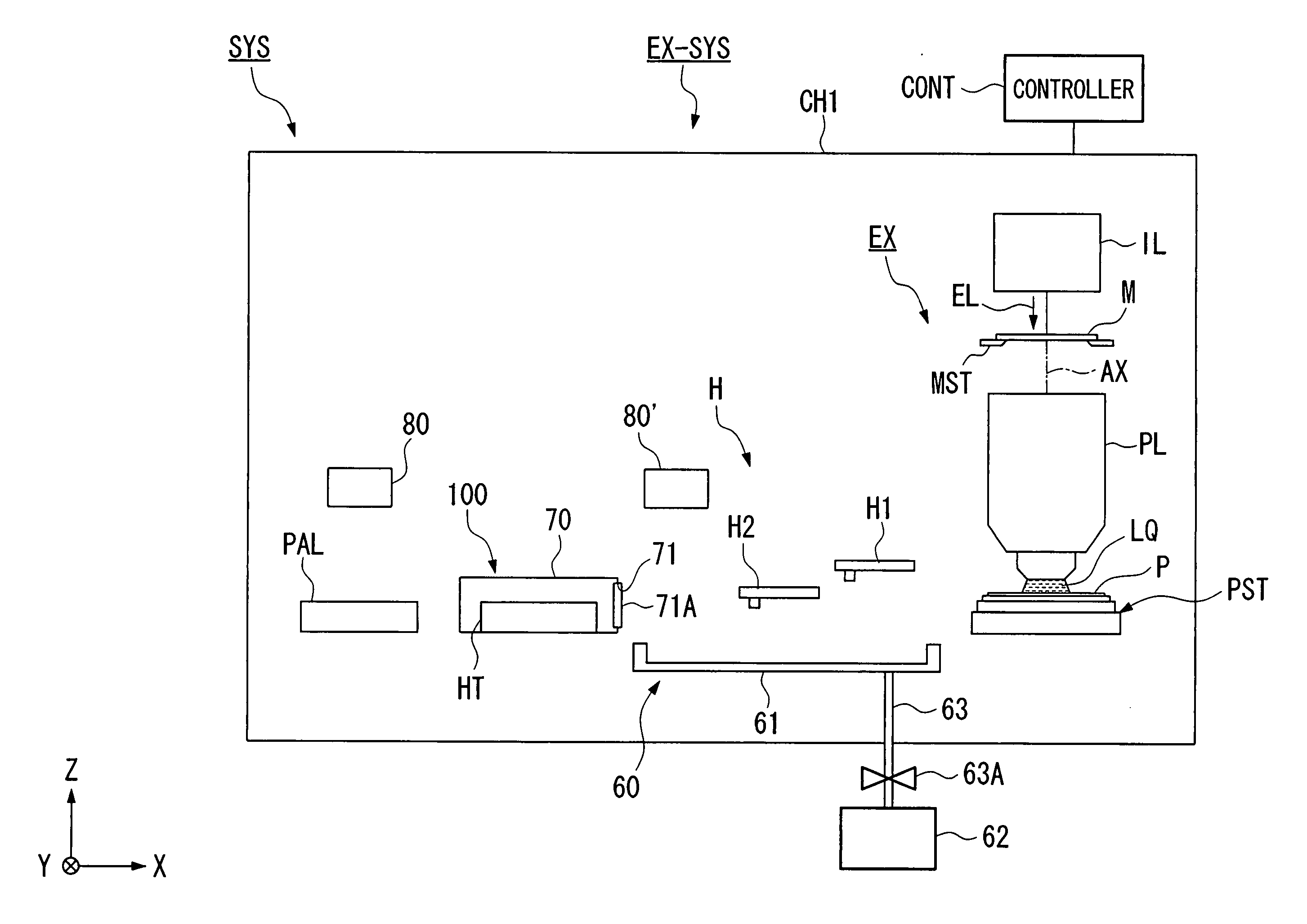
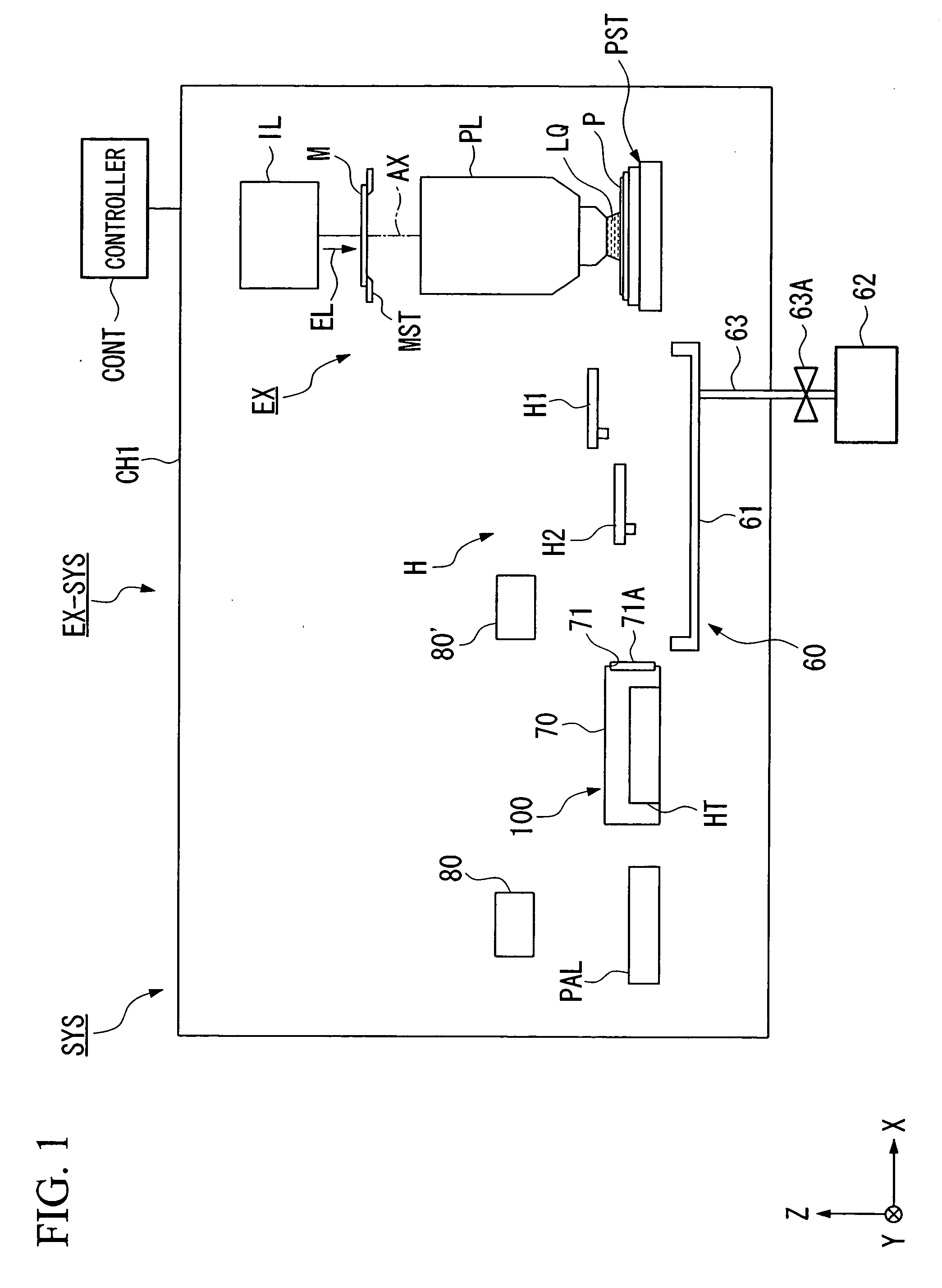
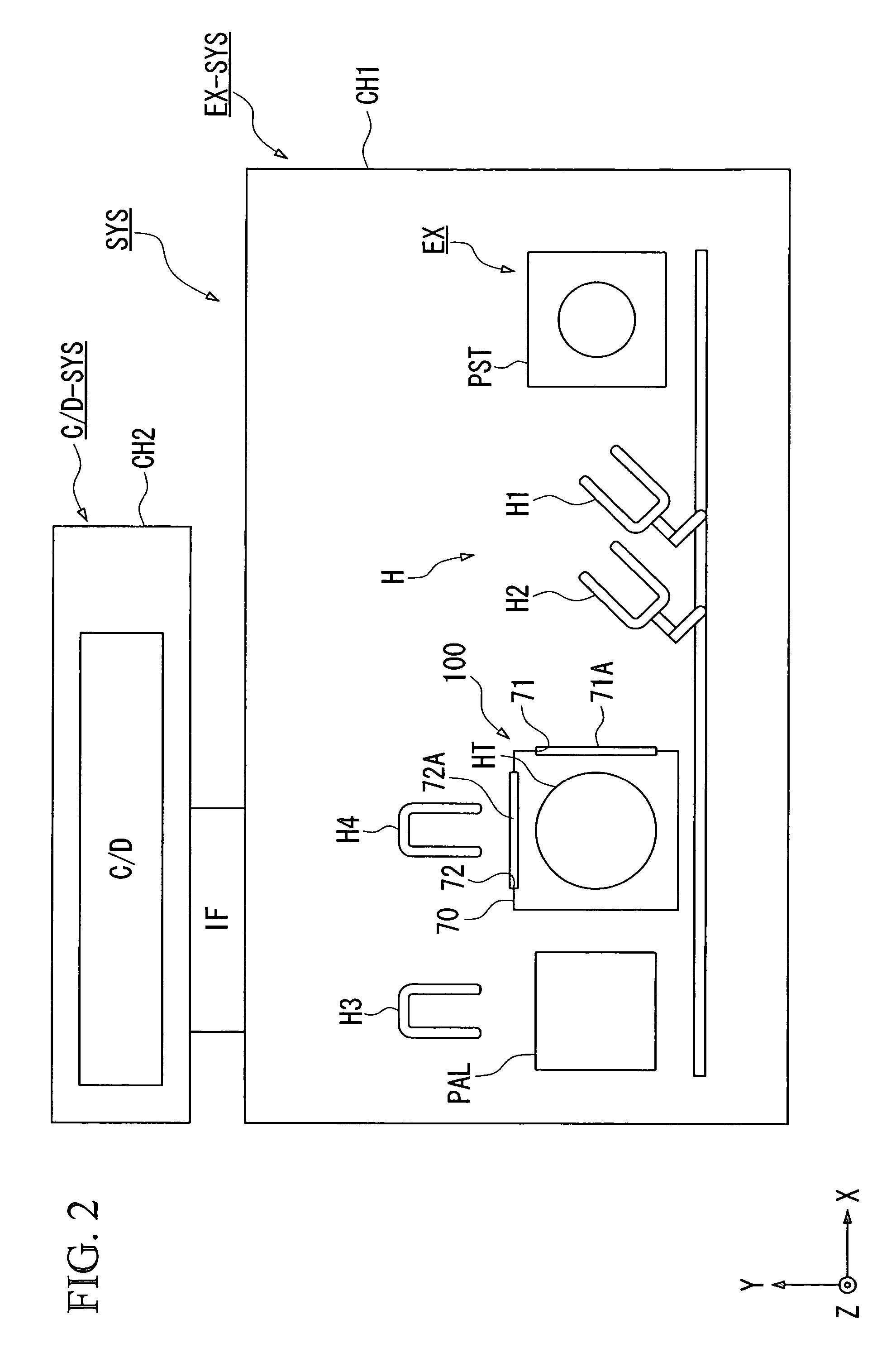
[0029] In the following, referring to the drawings, a substrate conveyance device and an exposure apparatus of the present invention will be described. FIG. 1 is a diagram showing an embodiment of a device manufacturing system provided with an exposure apparatus of the present invention and is a schematic diagram when viewed from the side; FIG. 2 is a diagram when FIG. 1 is viewed from above.

[0030] In FIGS. 1 and 2, device manufacturing system SYS is provided with exposure apparatus EX-SYS and coater-developer apparatus C / D-SYS (see FIG. 2). Exposure apparatus EX-SYS is provided with interface portion IF (see FIG. 2) that forms a connection portion thereof to coater-developer apparatus C / D-SYS, with exposure apparatus main body EX that by filling a space between projection optical system PL and substrate P with liquid LQ and by projecting a pattern formed on a mask onto substrate P via projection optical system PL and liquid LQ, exposes substrate P, with conveyance system H that co...


PUM

PropertyMeasurementUnit
Timeaaaaaaaaaa
Exposure limitaaaaaaaaaa
Optical reflectivityaaaaaaaaaa

Abstract

A substrate conveyance device that conveys a substrate having been exposed with a pattern image via a projection optical system and a liquid, the substrate conveyance device comprising: a liquid detector that detects the liquid adhering on the substrate.

Description

CROSS-REFERENCE TO RELATED APPLICATIONS [0001] This is a Continuation Application of International Application No. PCT / JP2004 / 014855 filed Oct. 7, 2004, which claims priority to 2003-349550. The contents of the aforementioned applications are incorporated herein by reference.BACKGROUND OF THE INVENTION [0002] 1. Field of the Invention [0003] The present invention relates to a substrate conveyance device and a substrate conveyance method that conveys a substrate exposed by a liquid immersion method, to an exposure apparatus and an exposure method, and to a device manufacturing method. [0004] The present application claims priority to Japanese Patent Application No. 2003-349550, filed on Oct. 8, 2003, and the content thereof is incorporated herein by reference. [0005] 2. Description of Related Art [0006] Semiconductor devices and liquid crystal display devices are manufactured through the so-called photolithography technique, by which a pattern formed on a mask is transferred onto a p...

Claims


Application Information

Patent Timeline
IPC IPC(8): C23C16/52B05C11/00G03F7/20H01L21/027
CPCG03B27/42G03D3/00G03F7/7075G03F7/70341G03F7/2041H01L21/0274H01L21/67709H01L21/67718G03F7/7085H01L21/677H01L21/67748H01L21/67751H01L21/0273
Inventor OHTA, ATSUSHIHORIUCHI, TAKASHI
Owner ZAO NIKON
Features
  • Generate Ideas
  • Intellectual Property
  • Life Sciences
  • Materials
  • Tech Scout
  • Unparalleled Data Quality
  • Higher Quality Content
  • 60% Fewer Hallucinations
Learn More