Apparatus and method for manufacturing a semiconductor wafer with reduced delamination and peeling

a technology of semiconductor wafers and manufacturing methods, applied in semiconductor/solid-state device testing/measurement, semiconductor devices, semiconductor/solid-state device details, etc., can solve problems such as cracks in low-k materials near die corners, damage is often introduced because of scribe lines, and achieve the effect of preventing delamination and peeling

Inactive Publication Date: 2006-11-23
TAIWAN SEMICON MFG CO LTD
View PDF5 Cites 229 Cited by
  • Summary
  • Abstract
  • Description
  • Claims
  • Application Information

AI Technical Summary

Benefits of technology

[0009] Accordingly, the present invention provides a “free area” that prohibits or substantially limits test key placement on the scribe lines in order to prevent delamination and peeling near the die corners.
[0010] The present invention also provides a conductive ring with one or more slots or rows of holes to prevent the low-k material from being cracked by stresses exerted at the die corners.

Problems solved by technology

Along with these advancements, the challenges of maintaining yield and throughput have also increased.
As far as reliability is concerned, the low-k material near die corners has a crack issue, especially in the sawing process.
Nevertheless, during wafer manufacture, damage is often introduced because of the scribe lines.
Consequently, portions of the wafer around the scribe line suffer damage, such as peeling, delamination, or dielectric fracture.
When considering a design rule for placement of test keys on the scribe line, major consideration is that the stress resulting from the sawing process causes serious peeling near the test keys at the die corners.
This results in delamination at the interface between the multiple layers at the die corners.
Delamination impacts the reliability of the device, and contributes to production of stringers (residual materials) that interfere with further processing and testing of the integrated circuit.
If a low-k material is used near the guard ring corners, the crack issue becomes more serious and further reduces reliability.

Method used


Image

  • Apparatus and method for manufacturing a semiconductor wafer with reduced delamination and peeling
  • Apparatus and method for manufacturing a semiconductor wafer with reduced delamination and peeling
  • Apparatus and method for manufacturing a semiconductor wafer with reduced delamination and peeling

Examples


Embodiment Construction

[0030] The making and using of embodiments of the present invention are discussed in detail below. It should be appreciated, however, that the present invention provides many applicable inventive concepts that can be embodied in a wide variety of specific contexts. The specific embodiments discussed are merely illustrative of specific ways to make and use the invention, and do not limit the scope of the invention.

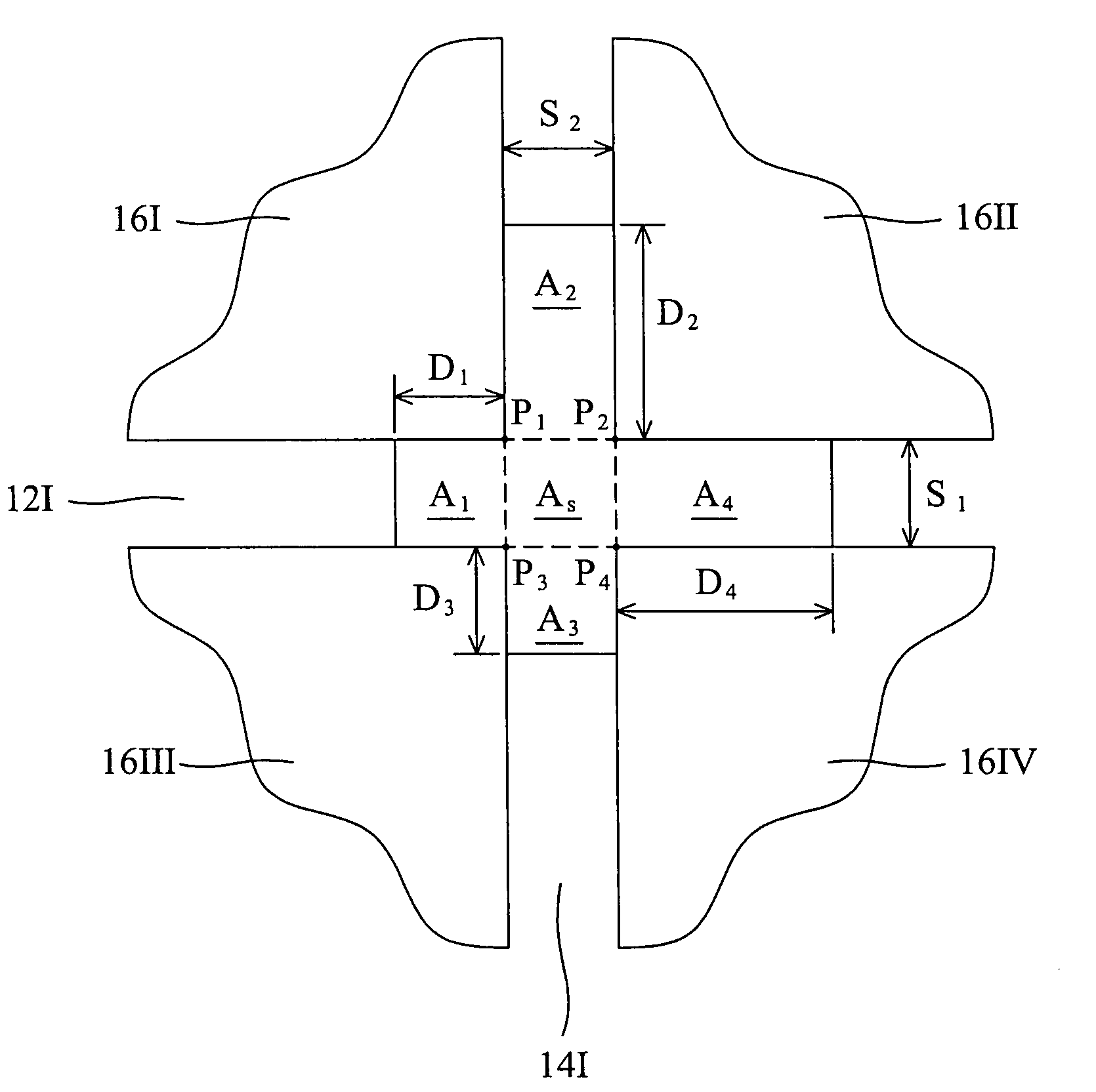
[0031] According to one embodiment of the present invention, a semiconductor wafer is provided with “free areas” that restrict the placement of test keys on scribe lines. This limitation or restriction reduces delamination or peeling near the die corners. The “free areas” located on the scribe lines may be used with an LK wafer (low-k wafer). Particularly, the phrase “free areas” restricting test key placement means that a limited arrangement of test keys may be placed or located in the “free area.” That is, a few test keys can be located on the free area if a measurement ...


PUM


Abstract

A multi-layered semiconductor structure with free areas limiting the placement of test keys. First and second scribe lines intersect to define one corner point of a die. The first and second scribe lines are part of the multilayered structure and at least one layer of the multi-layer structure is a low-k dielectric layer. Free area A1 is defined on the first scribe line and is defined by the equation A1=D1×S1, where D1 is the distance from the corner point of the die toward the main area of the die, and S1 is the width of the first scribe line. Free area AS is defined at the intersection of the first scribe line and the second scribe line adjacent the die and is defined by the equation AS=S1×S2, where S2 is the width of the second scribe line.

Description

[0001] This application is a continuation of U.S. patent application Ser. No. 10 / 675,862, entitled “Apparatus and Method for Manufacturing a Semiconductor Wafer with Reduced Delamination and Peeling,” filed on Sep. 30, 2003, which application claims the benefit of U.S. Provisional Application Ser. No. 60 / 462,969 filed on Apr. 15, 2003, entitled “Semiconductor Wafer with Free Areas for Test Key Placement,” both of which applications are hereby incorporated herein by reference.TECHNICAL FIELD [0002] The invention relates to a semiconductor wafer including an inter-metal-dielectric layer of low dielectric constant (low-k), and more particularly to a design rule for placing test keys on a scribe line. A second embodiment relates to a conductive ring design rule on a corner area of a die. A “free area” that restricts test key placement defined on the scribe line can prevent delamination or peeling near the die corners. One or more slots formed in the conductive ring can prevent the low-k...

Claims


Application Information

Patent Timeline
Patent Type & Authority Applications(United States)
IPC IPC(8): H01L23/52H01L21/301H01L23/544
CPCH01L22/34H01L2924/0002H01L2924/00
Inventor SU, CHAO-YUANTSAO, PEI-HAWLEE, HSIN-HUIHUANG, CHENDERHOU, SHANG Y.JENG, SHIN PUUTSAI, HAO-YIHU, CHENMING
Owner TAIWAN SEMICON MFG CO LTD
Why Eureka
Try Eureka