Voltage conversion circuit with stable transition delay characteristic

a voltage conversion circuit and transition delay technology, applied in logic circuits, pulse techniques, reliability increasing modifications, etc., can solve problems such as the generation of transfer signals (i.e. clock signals), distortion of duty ratio, and increase of leakage currents

Active Publication Date: 2006-11-23
SAMSUNG ELECTRONICS CO LTD
View PDF5 Cites 20 Cited by
  • Summary
  • Abstract
  • Description
  • Claims
  • Application Information

AI Technical Summary

Problems solved by technology

However, as the different voltages are applied to the functional blocks, leakage currents increase.
It therefore becomes difficult to ensure normal operational performance in interfacing with the functional blocks due to the resulting voltage differences between the external and internal voltages.
This produces generated distortions of transfer signals (i.e., clock signals) and duty ratio.
As is well known in the art, the distortion of the clock duty ratio causes a clock skew effect in the circuit.
The clock skew causes reduction of setup and hold margins.
In summary, the clock skew generation results in a decrease of operation speed and decreased performance in the level shifting circuit or voltage conversion circuit.

Method used


Image

  • Voltage conversion circuit with stable transition delay characteristic
  • Voltage conversion circuit with stable transition delay characteristic
  • Voltage conversion circuit with stable transition delay characteristic

Examples


second embodiment

[0070]FIG. 8 illustrates a type of voltage conversion circuit in the invention. The voltage conversion circuit 100 shown in FIG. 8 is substantially identical to that shown in FIG. 7, except the gate of the NMOS transistor M42 is connected to the node ND1 without the PMOS and NMOS transistors, M43 and M44. The circuit 100 of FIG. 8 operates in the same transition delay pattern and produces the same effect as that of FIG. 7, and therefore will not be discussed in further detail.

third embodiment

[0071]FIG. 9 illustrates a type of voltage conversion circuit in the invention.

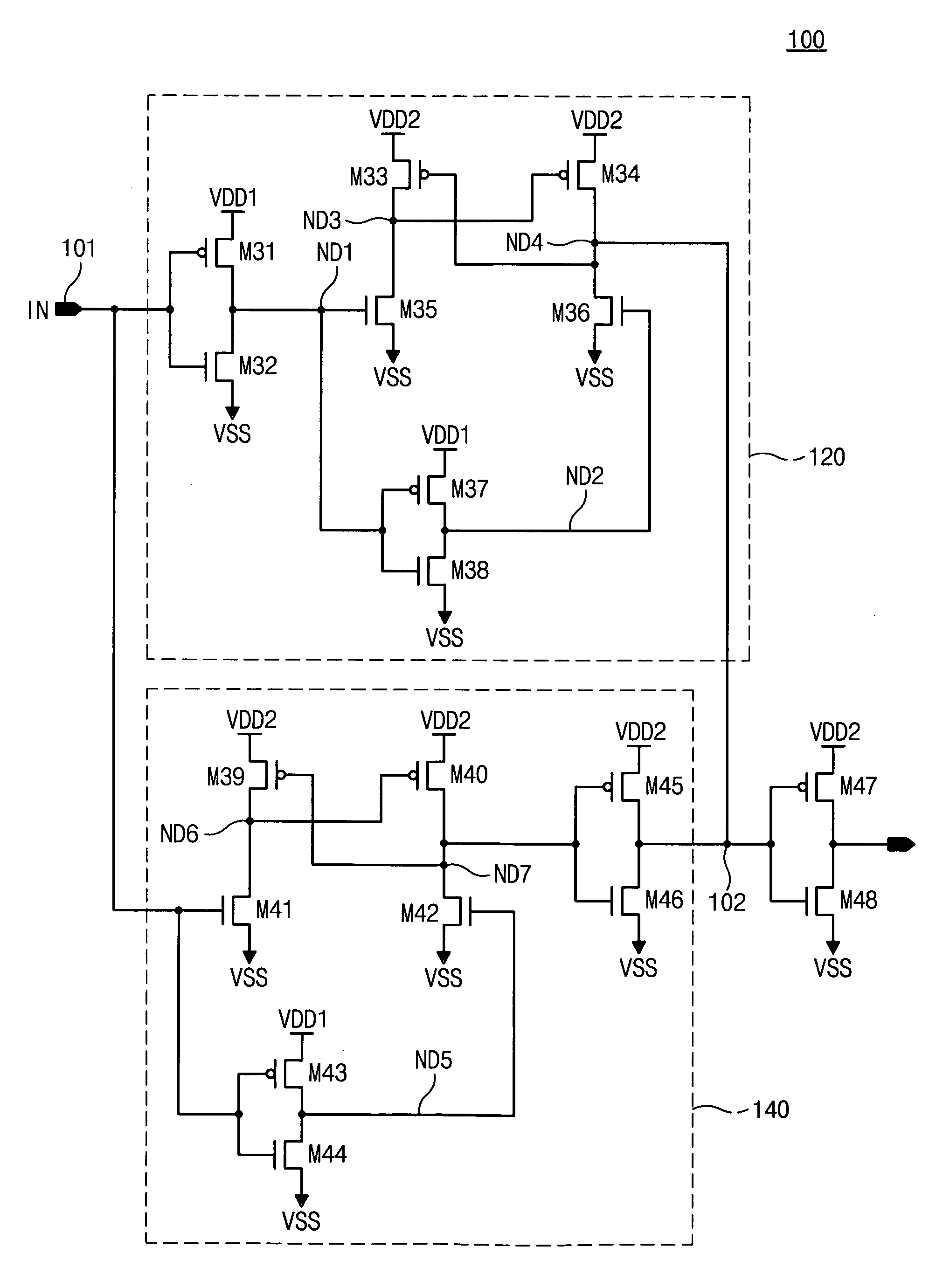
[0072] Referring to FIG. 9, the voltage conversion circuit 100 shown in FIG. 9 is substantially identical with that shown in FIG. 7, except for the additional PMOS and NMOS transistors, M49 and M50. The PMOS transistor M49 is composed of a gate coupled to the node ND1, a source connected to the second voltage VDD2, and a drain connected to the output terminal 102. The NMOS transistor M50 has a drain connected to the output terminal 102, a source grounded, and a gate coupled to the node ND2. The PMOS and NMOS transistors, M49 and M50, are provided to isolate the cross-coupling node, i.e., the node ND4, from the second level-shifting unit 140. In addition, the PMOS and NMOS transistors, M49 and M50, operate to pull-up and down a voltage level at the output terminal 102 in accordance with logic states of the nodes ND4 and ND1, which are the same as the functions of the PMOS and NMOS transistors M34 and M36. ...

fourth embodiment

[0073]FIG. 10 illustrates a type of voltage conversion circuit in the invention. The voltage conversion circuit 100 shown in FIG. 10 is substantially identical as that shown in FIG. 9, except that the gate of the NMOS transistor M42 is connected to the node ND1 without the PMOS and NMOS transistors M43 and M44. The circuit 100 of FIG. 10 operates in the same transition delay pattern and produces the same effect as that of FIG. 7, and therefore will not be discussed in further detail.


PUM


Abstract

A voltage conversion circuit changes an input signal of a first voltage into an output signal of a second voltage. The circuit includes an input terminal receiving an input signal, an output terminal generating an output signal, and first and second level-shifting units connected in parallel between the input and output terminals. The first and second level-shifting units have different transition delay characteristics, enabling rising and falling transition delays to be variable in the same ratio when the first and second voltages are changed.

Description

CROSS-REFERENCE TO RELATED APPLICATIONS [0001] This U.S. non-provisional patent application claims priority under 35 U.S.C. § 119 of Korean Patent Application 2005-42583 filed on May 20, 2005 and 2005-76246 filed on Aug. 19, 2005, the entire content of which is hereby incorporated by reference. BACKGROUND [0002] The disclosure herein is directed to integrated circuits, and more particularly, voltage conversion circuits in the form of integrated circuits. [0003] With the expansion of mobile product markets, there is additional need for power economization in the mobile devices because they must operate optimally for extended periods of time and with limited battery capacity. As a result, many techniques for power economization in mobile devices have been proposed. One proposal is to supply different voltages to functional blocks of the mobile apparatuses. In this configuration, low-functional blocks are supplied with lower voltages, and high-functional blocks are supplied with higher...

Claims


Application Information

Patent Timeline
Patent Type & Authority Applications(United States)
IPC IPC(8): H03K19/0175
CPCH03K3/011H03K19/00323H03K3/356113H03K3/0375
Inventor KIM, MIN-SU
Owner SAMSUNG ELECTRONICS CO LTD
Why Eureka
Try Eureka