System for identification of defects on circuits or other arrayed products

a technology of circuits and arrays, applied in the field of system and method for manufacturing products having arrays, can solve the problems of more defects that present an increased risk to the operation of a particular wafer, and achieve the effect of increasing the risk

Inactive Publication Date: 2006-11-23
IBM CORP
View PDF25 Cites 28 Cited by
  • Summary
  • Abstract
  • Description
  • Claims
  • Application Information

AI Technical Summary

Benefits of technology

[0009] Accordingly, one embodiment of the present invention is directed to a method for assessing a probability of failure to operation of a semiconductor wafer. This method includes inputting risk factor data into a memory and inputting a plurality of wafers into a semiconductor fabrication manufacturing process. Each wafer has at least one mask layer. A subset of wafers is selected to obtain a sample population and at least one region o

Problems solved by technology

One or more defects that present an increased risk to the operati

Method used


Image

  • System for identification of defects on circuits or other arrayed products
  • System for identification of defects on circuits or other arrayed products
  • System for identification of defects on circuits or other arrayed products

Examples


Embodiment Construction

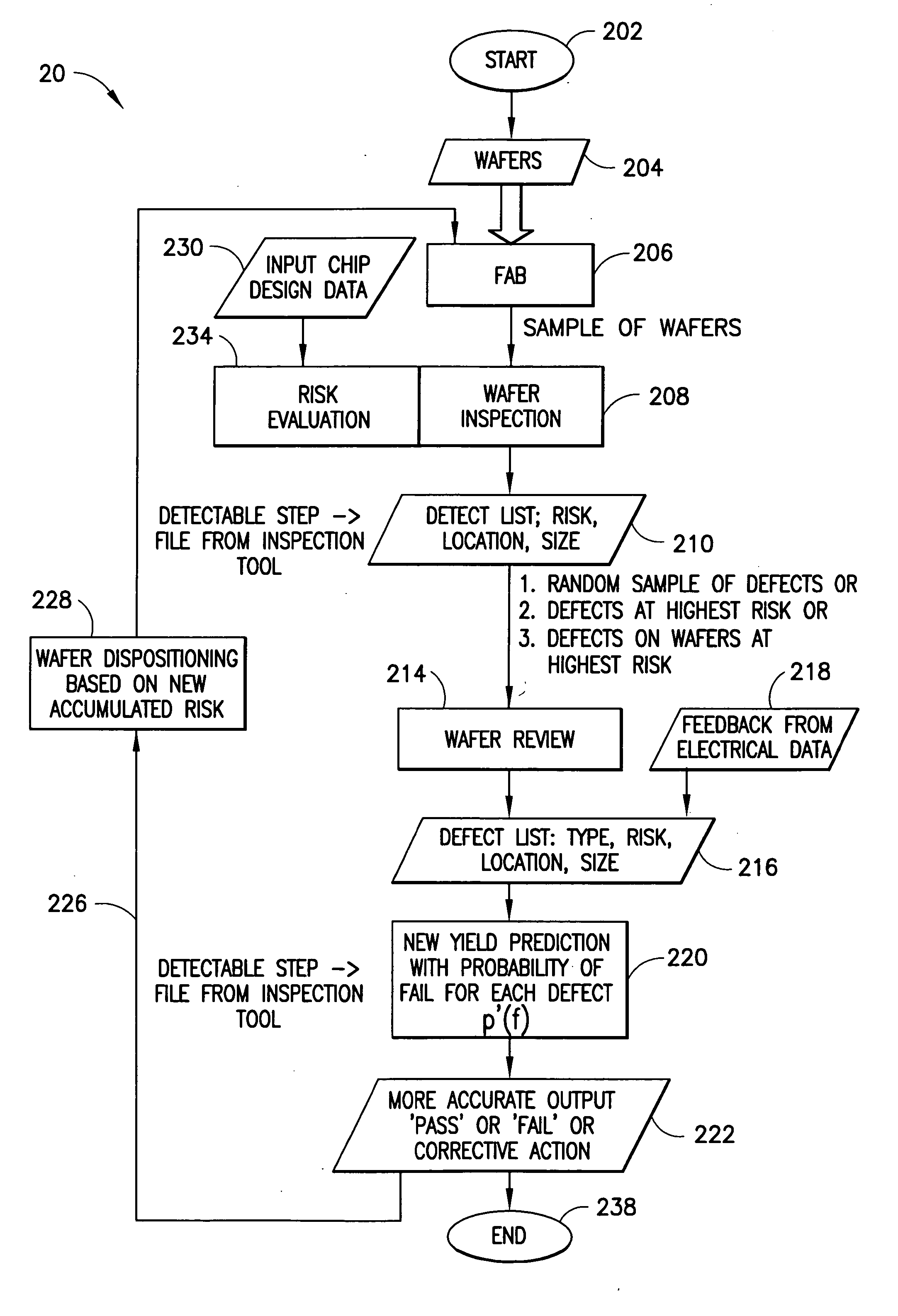
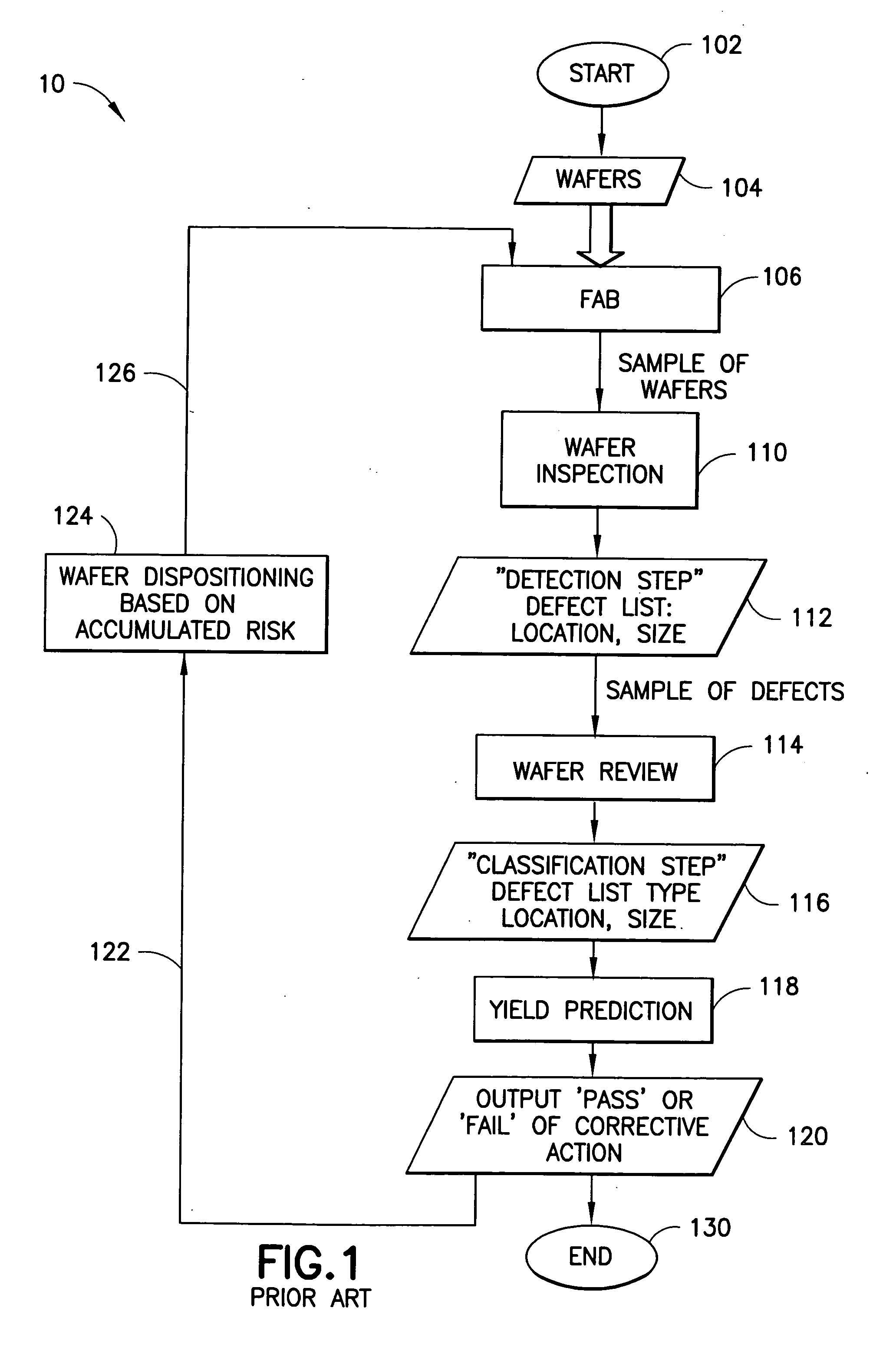
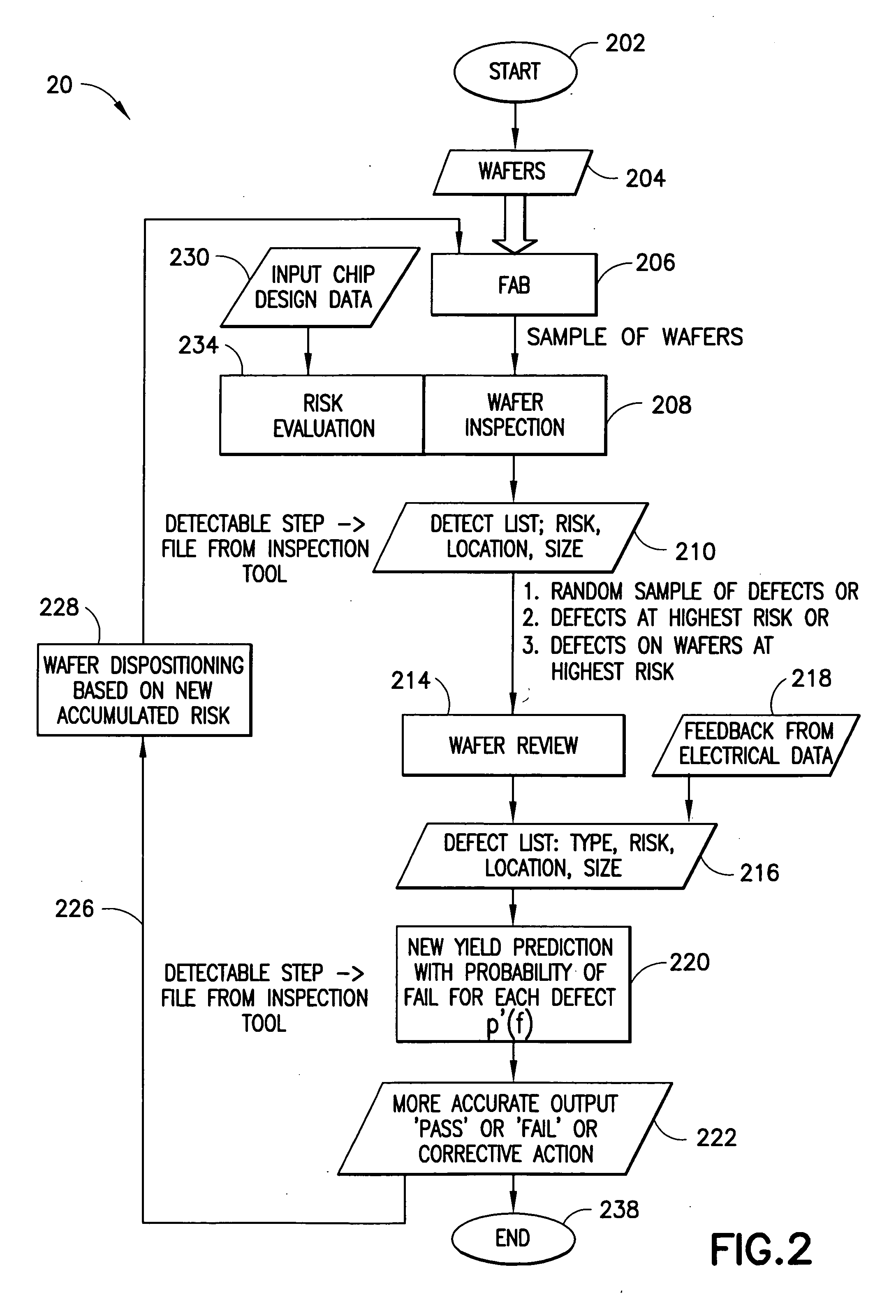
[0028] Semiconductor fabrication yield teams are continually challenged to increase yields. The lost revenue for each point of yield loss can be significant. In addition, the inspection process can be expensive and slow. Each tool has an associated Cost of Ownership (COO) which is driven by the capital cost of the tool and the tool's throughput. In order to increase yields there is a need to make better use of inspection resources. This can be accomplished by limiting the area inspected by high COO inspection tools, and by limiting the defects requiring review in high COO review tools.

[0029] The present invention is an improved system and method for identifying catastrophic or killer defects in semiconductor wafers and / or circuits, and identifying at risk semiconductor wafers and / or circuits, i.e., those wafers and / or circuits that exhibit an enhanced risk of catastrophic failure or inoperability. The present invention also applies to multi-layer semiconductor wafer and / or circuit ...


PUM


Abstract

A system and method is disclosed for assessing a probability of failure of operation of a semiconductor wafer. The method includes inputting risk factor data into a memory and inputting a plurality of wafers into a semiconductor fabrication manufacturing process. A subset of wafers is selected to obtain a sample population and at least one region of each wafer of the sample population is inspected. Circuit design data associated with each wafer of the sample population is obtained and one or more defects that present an increased risk to the operation of a particular wafer are identified. The identification is a function of the risk factor data, the inspecting step and the circuit design data. A probability of semiconductor wafer failure is calculated.

Description

FIELD OF THE INVENTION [0001] This invention relates generally to a system and method for manufacturing products having an array of sub-components, such as wafers and semiconductor circuits. More particularly, the present invention relates to efficiently identifying and characterizing defects in such products, improving yield and identifying yield trends. The present invention is particularly valuable in the fabrication of wafers and semiconductor circuits. BACKGROUND OF THE INVENTION [0002] In the semiconductor industry, there is a continuing movement towards higher integration, density and production yield, all without sacrificing throughput or processing speed. The fabrication of integrated circuits (ICs) requires a complex process to ensure the proper balance between throughput, processing speed and yield. Inspections and tests are designed to detect unwanted variations in the wafers produced, as well as in the equipment and masks used in the fabrication processes. One small def...

Claims


Application Information

Patent Timeline
IPC IPC(8): G06F17/18H01L21/66
CPCH01L22/20
Inventor LANZEROTTI, MARYYASHCHIN, EMMANUELLANDERS, CHRISTINATAKKEN, ASYATRAPP, BRIAN
Owner IBM CORP
Why Eureka
Try Eureka