Flat panel display device

a display device and flat panel technology, applied in the field of flat panel display devices, can solve the problems of lowering the performance of the display device, deteriorating the ability of the electrode, affecting etc., and achieves the effect of reducing unnecessary voltage drops, reducing the uniformity of image quality, and preventing the increase of electrode resistan

Inactive Publication Date: 2006-11-30
SAMSUNG SDI CO LTD
View PDF12 Cites 6 Cited by
  • Summary
  • Abstract
  • Description
  • Claims
  • Application Information

AI Technical Summary

Benefits of technology

[0012] An exemplary embodiment of the present invention provides a flat panel display device in which increase in electrode resistance may be prevented by forming an electrode protecting layer on a portion of an electrode passing through a sealing member which also eliminates unnecessary voltage drops and prevents a decrease in brightness and decrease in uniformity of image quality.

Problems solved by technology

Since the variation in composition of the metal film or the ITO film increases the inherent resistance thereof and the increase in resistance causes the voltage drop of the corresponding electrode, the abilities of the electrodes are deteriorated.
As a result, the flat panel display device is subjected to deterioration in image quality such as decrease in brightness and decrease in uniformity of brightness due to deterioration in ability of the electrodes, thereby lowering the performance of the display device.

Method used


Image

  • Flat panel display device
  • Flat panel display device
  • Flat panel display device

Examples


Embodiment Construction

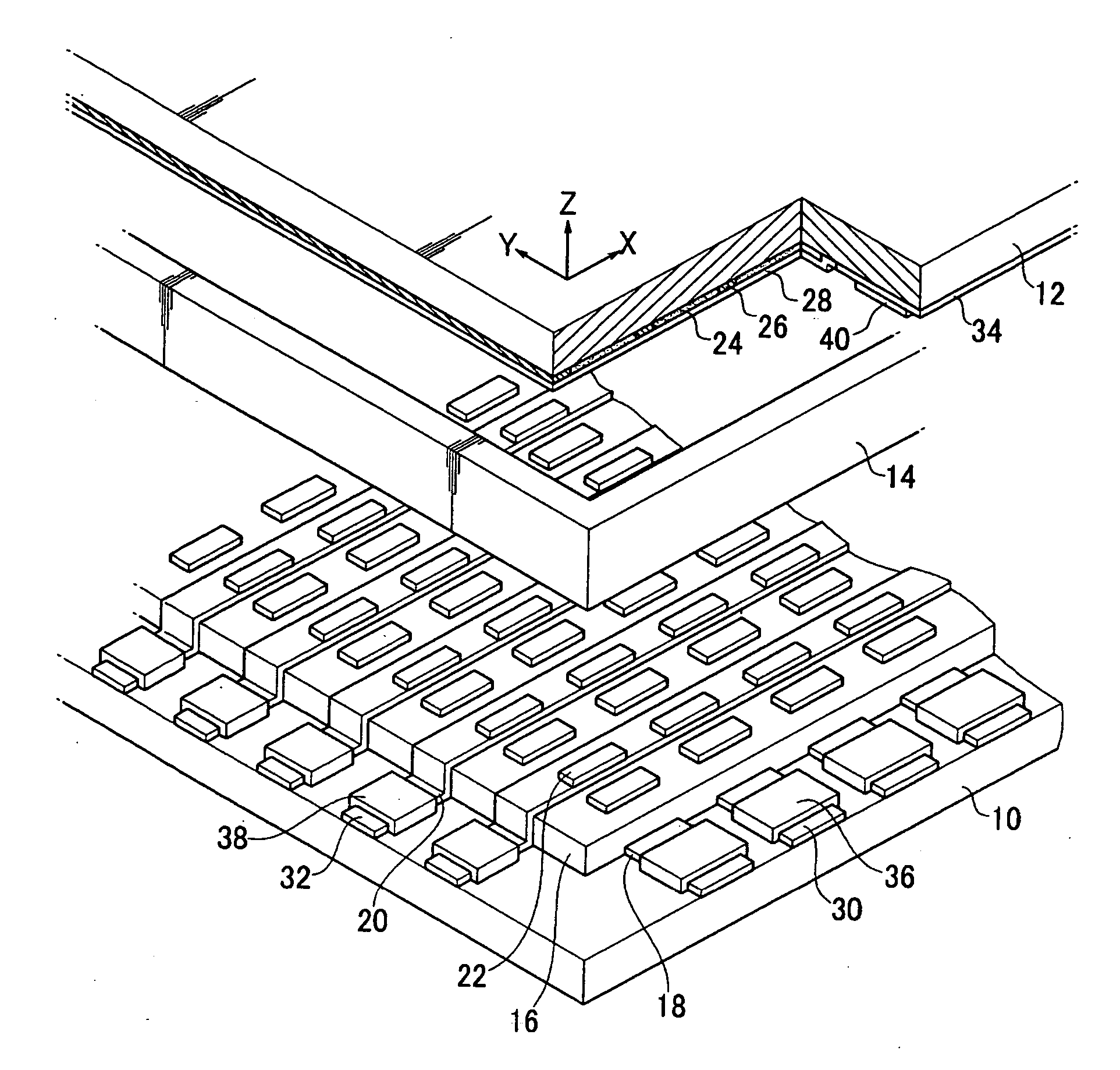
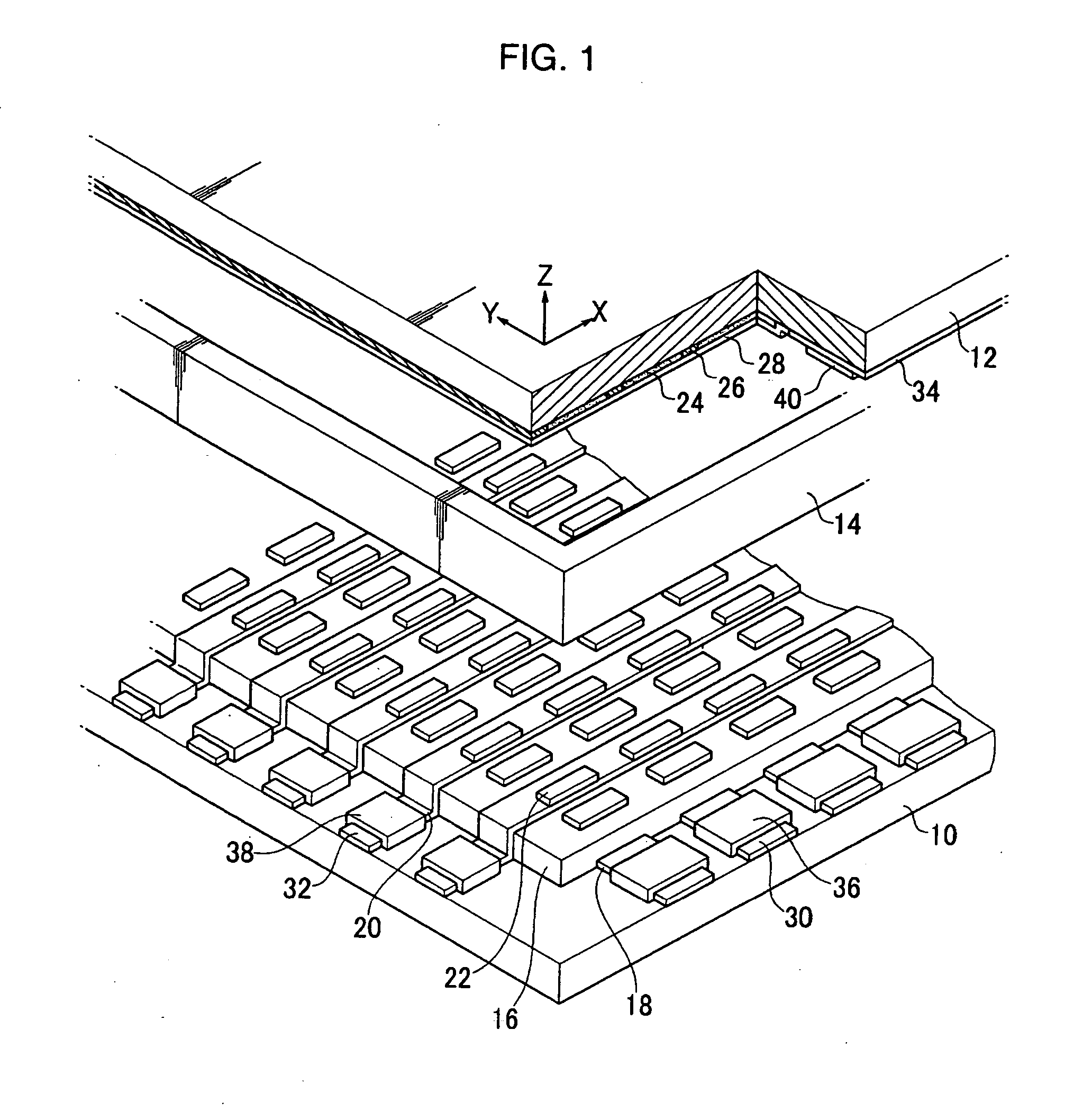
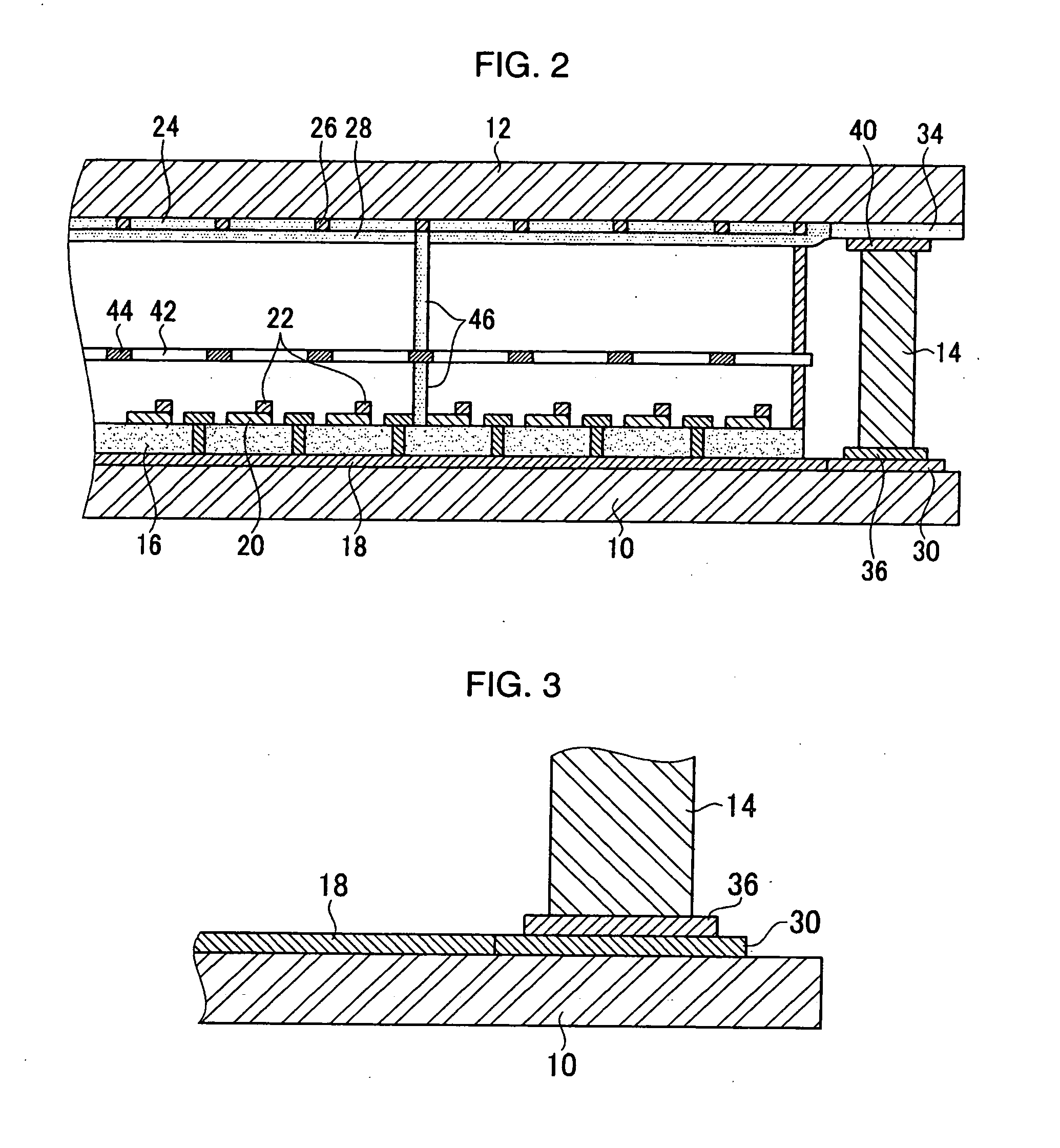
[0030] According to one embodiment of the present invention, an FEA type field emission device is shown in FIGS. 1 and 2. The field emission device includes a first substrate 10 and a second substrate 12 disposed to oppose each other with a predetermined gap therebetween. A sealing member 14 is disposed between the circumferential edges of the first substrate 10 and the second substrate 12 which seals the substrates. Gate electrodes 18 and cathode electrodes 20 are formed in a pattern intersecting each other on the first substrate 10 with an insulating layer 16 therebetween. Electron emission regions 22 are formed on the portions of the cathode electrodes 20 intersecting the gate electrodes 18.

[0031] The field emission device also includes fluorescent film 24 formed on the second substrate 12, black film 26 disposed between the fluorescent film 24, and an anode electrode 28 formed on the second substrate 12 to cover the fluorescent film 24 and the black film 26. In the present embo...


PUM

PropertyMeasurementUnit
temperatureaaaaaaaaaa
electric fieldaaaaaaaaaa
conductiveaaaaaaaaaa

Abstract

A flat panel display device includes a first substrate and a second substrate disposed to oppose each other with a predetermined gap therebetween. An electrode made of a conductive film is formed on at least one of the first substrate and the second substrate. A sealing member is disposed between the first substrate and the second substrate and bonds the first substrate and the second substrate to each other. An electrode protecting layer is formed on a portion of the electrode overlapping with the sealing member and between the sealing member and the electrode. The electrode and the electrode protecting layer may be made of a conductive metal.

Description

CROSS REFERENCE TO RELATED APPLICATIONS [0001] This application is a continuation-in-part application of U.S. patent application Ser. No. 11 / 046,503 filed on Jan. 28, 2005, which in turn claims priority to and the benefit of Korean Patent Application No. 10-2004-0005969 filed on Jan. 30, 2004 in the Korean Intellectual Property Office, the entire content of both of which are incorporated herein by reference.BACKGROUND OF THE INVENTION [0002] 1. Field of the Invention [0003] The present invention relates to a flat panel display device, and more particularly, to a flat panel display device in which an increase in electrode resistance may be prevented. [0004] 2. Description of the Related Art [0005] In flat panel display devices, such as the field emission display (FED), the vacuum fluorescent display (VFD), the lliquid crystal display (LCD), and the plasma display panel (PDP), an upper substrate and a lower substrate are disposed with a predetermined gap, and a vacuum vessel is formed...

Claims


Application Information

Patent Timeline
Patent Type & Authority Applications(United States)
IPC IPC(8): H01J63/04H01J1/62G02F1/1345G02F1/1339G09F9/00G09F9/30H01J1/05H01J1/14H01J5/32H01J9/04H01J9/12H01J17/18H01J29/86H01J29/90H01J29/92H01J31/12H01L27/32H01L51/52
CPCG02F1/1345H01J5/32H01J17/18H01L51/5237H01J29/90H01L27/3281H01L51/5206H01J29/86H10K59/179H10K50/81H10K50/8426H10K50/844B23Q3/062
Inventor CHI, EUNG-JOON
Owner SAMSUNG SDI CO LTD
Why Eureka
Try Eureka