

Program method of flash memory device
- Summary
- Abstract
- Description
- Claims
- Application Information
AI Technical Summary
Benefits of technology
Problems solved by technology
Method used
Image

Examples
Embodiment Construction
[0034] Embodiments in accordance with the present invention will be described with reference to the accompanying drawings.
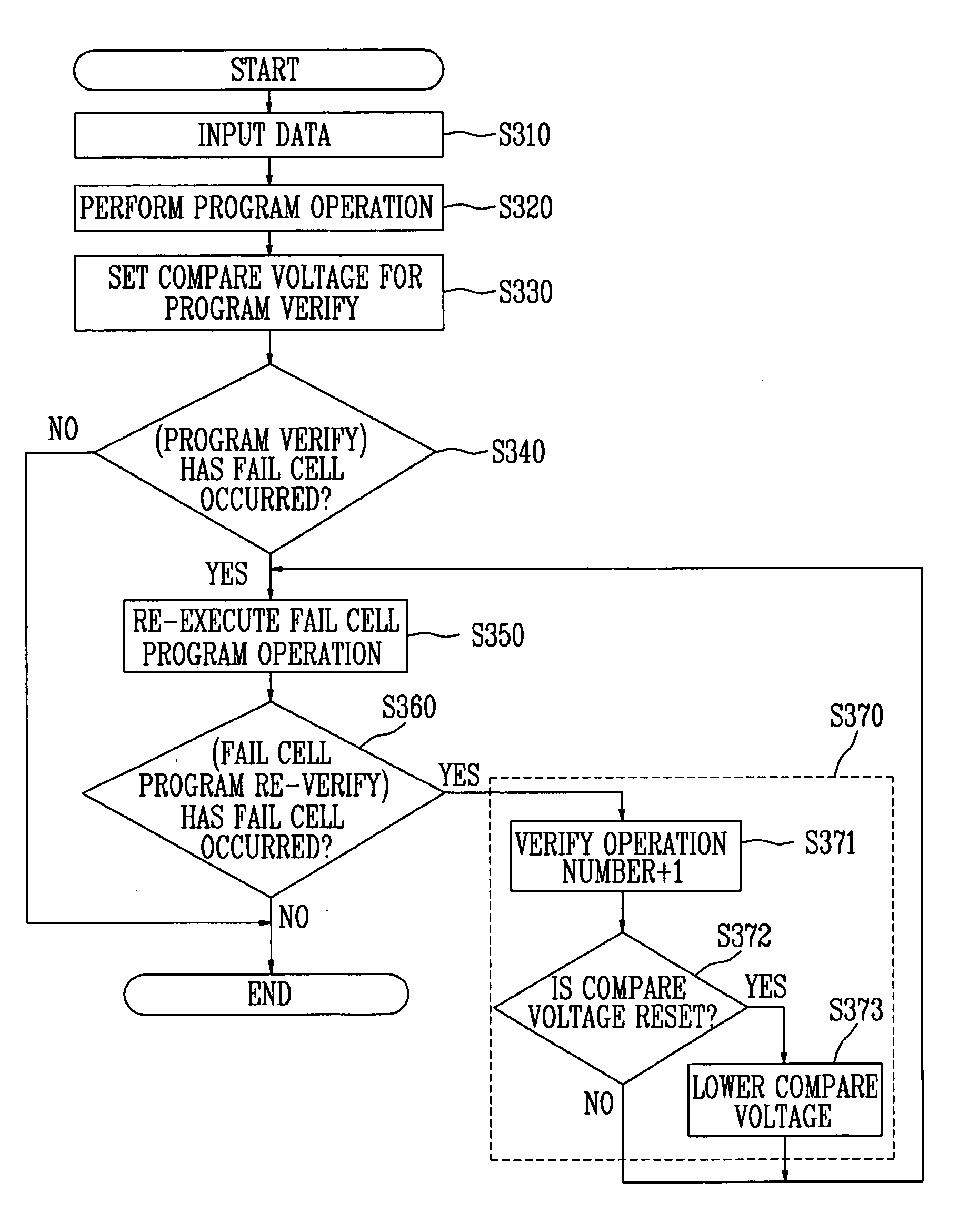
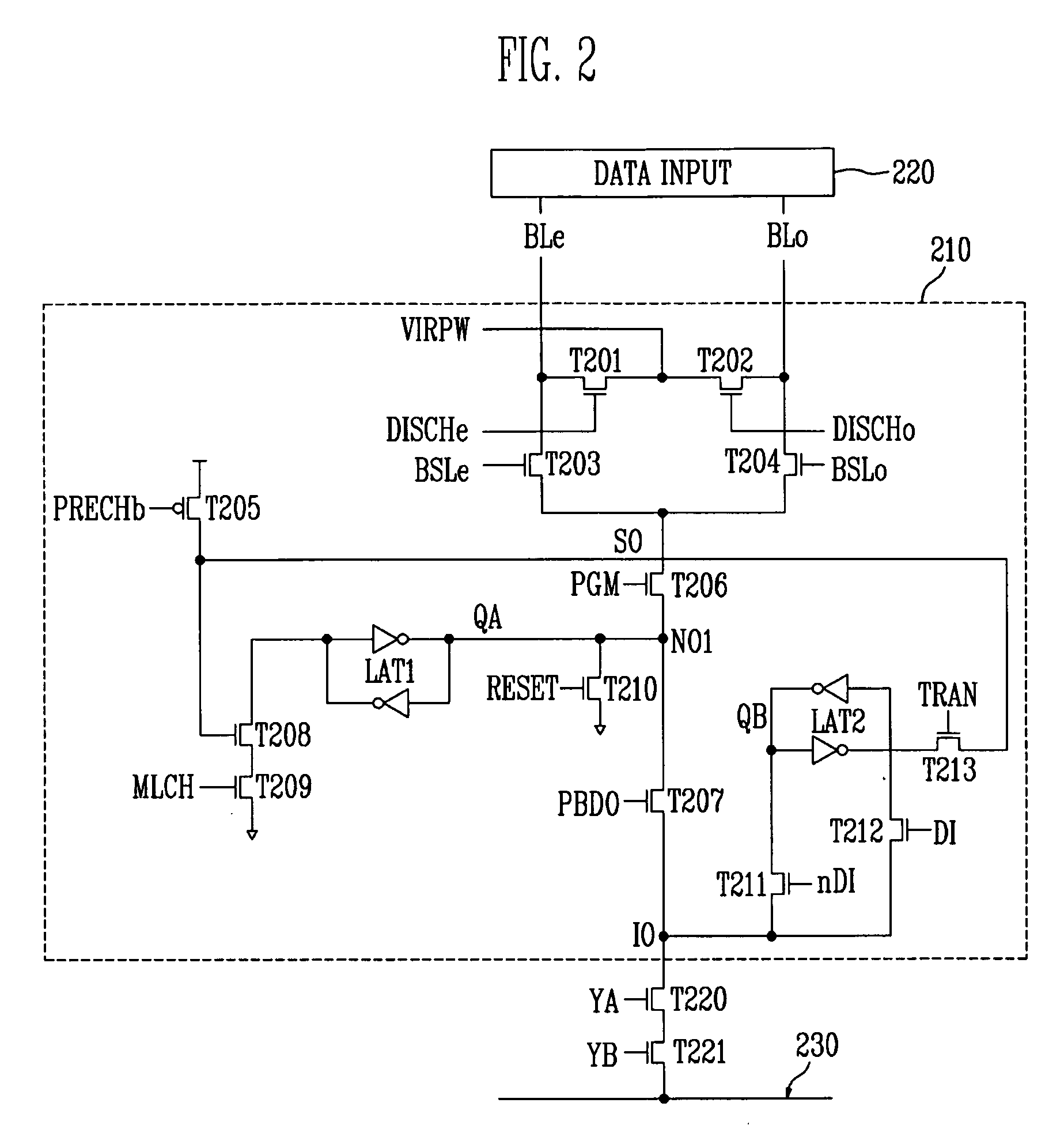
[0035]FIG. 2 is a circuit diagram of a page buffer included in a NAND-type flash memory device. FIG. 3 is a flowchart illustrating steps embodying a method of programming a flash memory device according to an embodiment of the present invention.
[0036] Referring to FIG. 2, the page buffer 210 is connected to bit lines BLe and BLo of a memory cell array 220 having a plurality of memory cells. Transistors T220 and T221 for electrically connecting the page buffer 210 and a data line 230 according to signals (YA and YB) generated depending on column address information are connected between the page buffer 210 and the data line 230.
[0037] Constituent elements of the page buffer 210 will be described in detail below.
[0038] A bias circuit is connected between the even bit line BLe and the odd bit line BLo. The bias circuit includes first and second transistors T201 ...
PUM
 Abstract
Description
Claims
Application Information