Pixel individual anti-eclipse circuit and its operation manner

a technology of anti-eclipsing circuit and pixel, applied in the field of semiconductor imagers, can solve the problems of reducing vref voltage and difficulty in obtaining a sufficient output level for anti-eclipsing

Active Publication Date: 2006-12-14
APTINA IMAGING CORP
View PDF13 Cites 28 Cited by
  • Summary
  • Abstract
  • Description
  • Claims
  • Application Information

AI Technical Summary

Benefits of technology

[0013] Exemplary embodiments of the invention provide an anti-eclipse circuit, and method of forming the same, comprising a pixel coupled to a pixel output line and a circuit for receiving and storing a pixel reset voltage from the pixel on the pixel output line and for using the stored pixel reset voltage as a parameter to control a reset voltage level on the output line in a manner which maintains the pixel reset voltage on the pixel output line above a predetermined minimum voltage.

Problems solved by technology

One limitation of the anti-eclipse circuit 230 is to have a sufficient margin against possible variations of VRST.
Therefore, VREF should be chosen as a sufficiently low voltage supposing a minimum value VRST variation, which results in reduced VREF voltage and causes difficulty in obtaining a sufficient output level for anti-eclipsing.

Method used


Image

  • Pixel individual anti-eclipse circuit and its operation manner
  • Pixel individual anti-eclipse circuit and its operation manner
  • Pixel individual anti-eclipse circuit and its operation manner

Examples


first embodiment

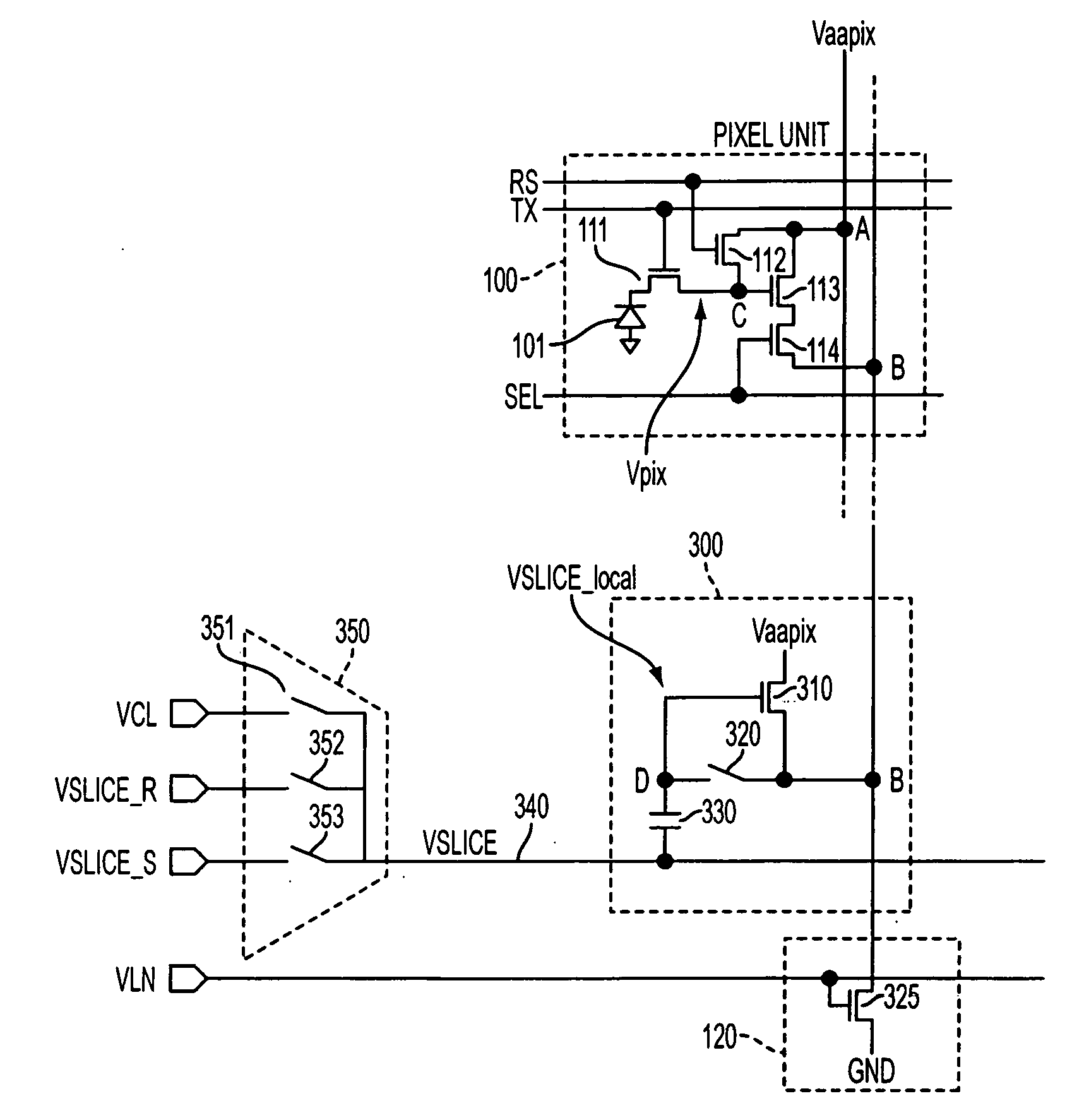
[0024] Now referring to the figures, where like numerals designate like elements, FIG. 3A shows the invention, which includes pixel circuit 100, a clip circuit 300, and a global multiplex circuit 350. Pixel circuit 100 is the same as that described in connection with FIG. 1. Clip circuit 300 includes a clip transistor 310, a clamp switch 320, a memory capacitor 330, and VSLICE_local node D. Global multiplex circuit 350 includes a first control switch 351, a second control switch 352, and a third control switch 353. Clip circuit 300 is connected to pixel 100 at node B. Clip transistor 310 is connected at its drain to Vaapix (node A), and at its source is coupled to the first terminal of clamp switch 320 and thus to a column line of an imager. The gate of clip transistor 310 is coupled to VSLICE_local node D. The second terminal of clamp switch 320 is also connected to node D. Memory capacitor 330 is coupled at one terminal to node D. The other terminal of memory capacitor 330 is conn...

second embodiment

[0032]FIG. 3B illustrates the invention. In comparison with FIG. 3A, a Vaapix enable transistor 360 is additionally implemented in clip circuit 300′. Vaapix enable switch 360 may be very small, as it is used to charge memory capacitor 330. Also, the location of clamp switch 320 is changed to the drain side of the clip transistor 310.

[0033]FIG. 4B describes the an exemplary operation of the embodiment illustrated in FIG. 3B and shows the resulting VRST signal during circuit operation. At time t0, row select signal SEL is applied to the pixel 100 so that the pixel 100 is selected. Reset signal RS is pulsed and charging signal SLICE_EN_BAR is deasserted at time t1. Since the signal CL is pulsed, node D is connected with the Vaapix through Vaapix enable transistor 360 at this time. At time t1a, charging signal SLICE_EN_BAR is asserted and the Vslice_local node D and drain node of clip transistor 310 are both disconnected from Vaapix, so that the Vslice_local voltage decreases with the c...

third embodiment

[0037]FIG. 3C shows the invention. In comparison with the configuration of the embodiment shown in FIG. 3B, a DC current switch 370 is introduced between clip transistor 310 and Vpixout node B in clip circuit 300″. Second switch 370 is kept open when the drain voltage of clip transistor 310 is driven to Vaapix, so that no DC current flows during the charge up period of memory capacitor 330.

[0038]FIG. 4C describes the an exemplary operation of the embodiment illustrated in FIG. 3C. The operation is the same as that described in FIG. 4B, with an additional signal SLICE_EN2 that controls DC current switch 370. SLICE_EN2 is asserted at time t1a at the same time SLICE_EN_BAR is asserted, and SLICE_EN2 is deasserted at time t7 when SLICE_EN_BAR in reasserted. This causes the voltage at node B to stay at VRST from time t1 to time t1a to avoid affecting the sampled reset voltage.

[0039] Each imager may also be arranged in an array, or as part of a processing system. Clip circuit 300 and glo...


PUM


Abstract

An anti-eclipse circuit of an image pixel includes a pixel coupled to a pixel output line and a circuit for receiving and storing a pixel reset voltage from the pixel on the pixel output line and for using the stored pixel reset voltage as a parameter to control a reset voltage level on the output line in a manner which maintains the pixel reset voltage on the pixel output line above a predetermined minimum voltage.

Description

FIELD OF INVENTION [0001] The present invention relates generally to semiconductor imagers. More specifically, the present invention relates to an anti-eclipse circuit for imagers. BACKGROUND OF THE INVENTION [0002] A CMOS imager circuit includes a focal plane array of pixel cells, each one of the cells including a photosensor, for example, a photogate, photoconductor or a photodiode for accumulating photo-generated charge in a specified portion of a substrate. Each pixel cell has a charge storage region, formed on or in the substrate, which is connected to the gate of an output transistor that is part of a readout circuit. The charge storage region may be constructed as a floating diffusion region. In some imager circuits, each pixel may include at least one electronic device such as a transistor for transferring charge from the photosensor to the storage region and one device, also typically a transistor, for resetting the storage region to a predetermined charge level prior to ch...

Claims


Application Information

Patent Timeline
Patent Type & Authority Applications(United States)
IPC IPC(8): H01L27/00H01L27/146H04N5/335H04N5/369H04N5/372H04N5/376H04N5/378
CPCH04N5/3598H04N25/627H04N25/40H04N25/76
Inventor TAKAYANAGI, ISAO
Owner APTINA IMAGING CORP
Why Eureka
Try Eureka