Abnormality cause specifying method, abnormality cause specifying system, and semiconductor device fabrication method

a technology of abnormality and specifying system, applied in semiconductor/solid-state device testing/measurement, testing/monitoring control system, instruments, etc., can solve problems such as inability to specify data amount huge, and general difficulty in defining abnormality causes of defective products

Inactive Publication Date: 2006-12-14
KK TOSHIBA
View PDF3 Cites 30 Cited by
  • Summary
  • Abstract
  • Description
  • Claims
  • Application Information

AI Technical Summary

Problems solved by technology

Once a defective LSI is produced, therefore, it is generally very difficult to specify the abnormality cause of the defective product.
Of these distributions, the clustering defect distribution is in many cases caused by the process, fabrication apparatus, or the like as an abnormality cause.
That is, if an abnormality occurs in a certain process or fabrication apparatus, defective products having a clustering defect distribution unique to the process or fabrication apparatus are produced.
Unfortunately, there are hundreds of semiconductor device fabrication steps.
To make it possible to specify an abnormality cause in each individual fabrication step, therefore, it is necessary to acquire various data in these fabrication steps and in inspection steps before and after the fabrication steps, and this makes the data amount enormous.
The enormous data makes it very difficult to select data which is truly significant to specify an abnormality cause, thereby making specification of an abnormality cause impossible.

Method used


Image

  • Abnormality cause specifying method, abnormality cause specifying system, and semiconductor device fabrication method
  • Abnormality cause specifying method, abnormality cause specifying system, and semiconductor device fabrication method
  • Abnormality cause specifying method, abnormality cause specifying system, and semiconductor device fabrication method

Examples


first embodiment

(Semiconductor Device Fabrication System)

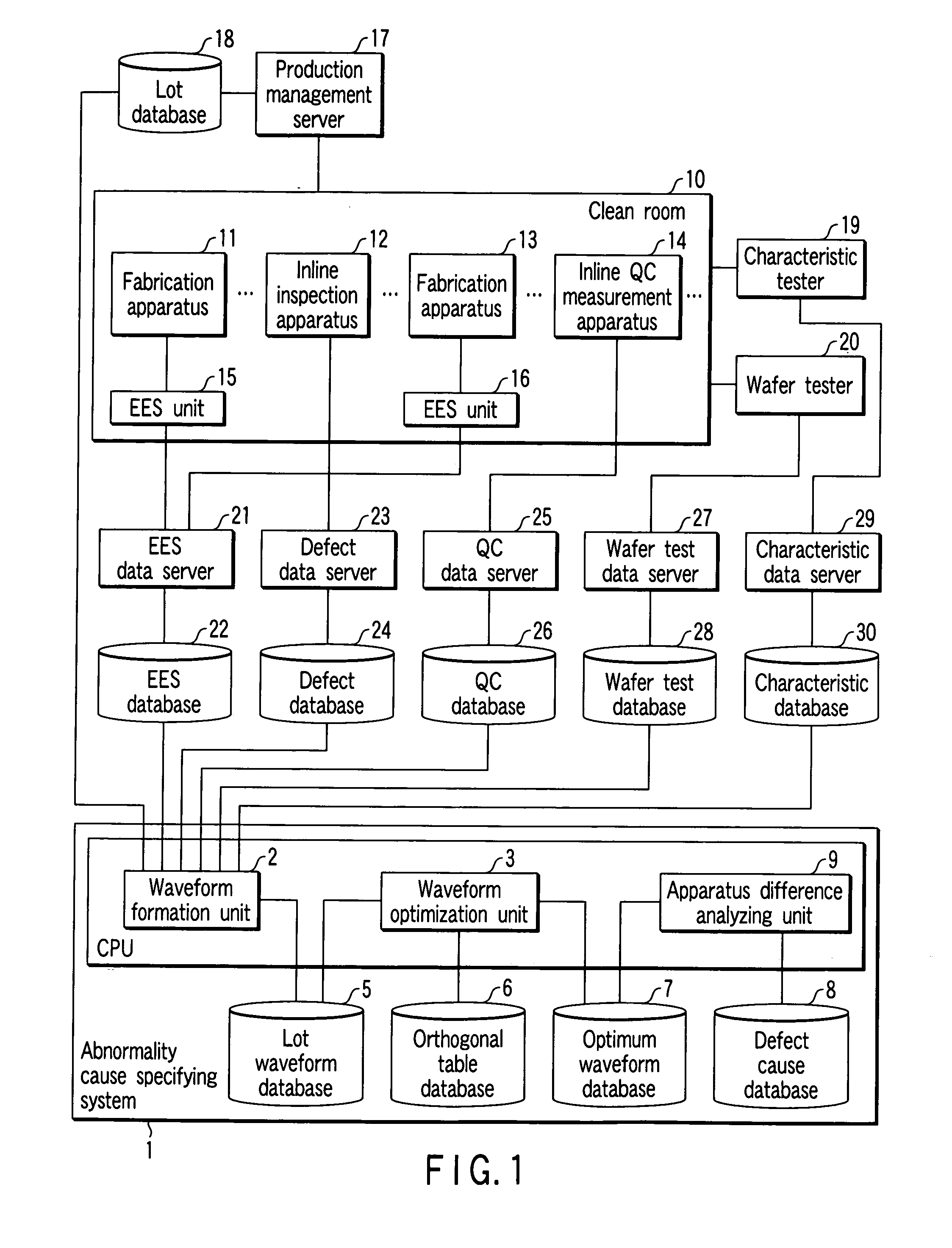
[0036] As shown in FIG. 1, a semiconductor device fabrication system has a clean room 10 which includes fabrication apparatuses 11 and 13, an inline inspection apparatus 12, an inline quality control (QC) measurement apparatus 14, and equipment engineering systems (EESs) 15 and 16 connected to the fabrication apparatuses 11 and 13, respectively.

[0037] To fabricate semiconductor devices, the fabrication apparatuses 11 and 13 perform processing of semiconductor wafers forming lots under various operating conditions, and the states of semiconductor devices momentarily change in accordance with the processing. The device state can be represented by any of various physical amounts such as the internal pressure, gas flow rate, and temperature of a chamber, and the exposure amount of an exposure apparatus. Data of these physical amounts at each time is called EES data. The EES data can be obtained by attaching the EES units 15 and 16 for monitori...

second embodiment

[0112] In the first embodiment, whether to adopt waveform data is selected for all types of waveform data by using a two-level orthogonal table. However, it is also possible to perform selection beforehand so that specific waveform data is always selected as in the second embodiment. For example, assume that there is a clustering defect by which a number of defective chips are produced in the wafer center in a wafer test, and there are a plurality of causes for the same clustering defect in the wafer center.

[0113] In the first embodiment, a wafer center defective lot group Sc is formed using only waveform data of the wafer test. However, the cause of the defect cannot be specified even when apparatus difference analysis is performed on the wafer center defective lot group Sc.

[0114] In the second embodiment, therefore, wafer test data is always adopted in any trial when waveform data is to be selected by using an orthogonal table. In addition, when an optimum similar lot group Sco ...

third embodiment

[0115] In the third embodiment, a method which immediately detects an abnormality in a fabrication step and controls the detected fabrication step by using only a waveform data group acquired in semiconductor device fabrication steps will be described. Data acquired in semiconductor device fabrication steps is called inline data, and examples of the inline data are defect data, EES data, and QC data. The semiconductor device fabrication method of the first embodiment was exclusively applied to the inline data. Consequently, in an optimum similar lot set using an optimum waveform data set obtained by connecting waveform data of defect map data of fabrication step C shown in FIG. 20A and waveform data of chamber pressure data of a fabrication apparatus in fabrication step C shown in FIG. 20B, a large abnormality degree was detected in a specific fabrication apparatus in fabrication step C. When defect map data in fabrication step C of wafers in lots forming the optimum similar lot set...


PUM


Abstract

A feature amount is generated by standardizing inspection data related to a fabrication unit for each type, a similar set including fabrication units corresponding to similar feature amounts is formed by comparing the feature amounts, and apparatus difference analysis is performed between a plurality of fabrication units forming the similar set. A two-level orthogonal table is used to determine whether to adopt a feature amount of each type, and some feature amounts are not used in the apparatus difference analysis and the like by optimizing the smaller-the-better characteristic or the larger-the-better characteristic of a test value of the apparatus difference analysis, thereby reducing the calculation amount and accurately and efficiently specifying an abnormality cause.

Description

CROSS-REFERENCE TO RELATED APPLICATIONS [0001] This application is based upon and claims the benefit of priority from prior Japanese Patent Application No. 2005-174137, filed Jun. 14, 2005, the entire contents of which are incorporated herein by reference. BACKGROUND OF THE INVENTION [0002] 1. Field of the Invention [0003] The present invention relates to a method and system of specifying an abnormality cause in the fabrication process of a product, and a semiconductor device fabrication method. [0004] 2. Description of the Related Art [0005] One of the largest problems to be solved to increase the productivity of products, e.g., semiconductor devices is to increase the yield. To increase the yield, it is important to analyze the yield loss, and find and improve the process, fabrication apparatus, or design condition which is used in the fabrication process having caused the loss, in the early stages. However, semiconductor devices, particularly, semiconductor integrated circuits (L...

Claims


Application Information

Patent Timeline
Patent Type & Authority Applications(United States)
IPC IPC(8): H01L21/66G01R31/26
CPCG05B23/024H01L22/20
Inventor MATSUSHITA, HIROSHI
Owner KK TOSHIBA
Why Eureka
Try Eureka