Memory device and method of controlling operation of the memory device
- Summary
- Abstract
- Description
- Claims
- Application Information
AI Technical Summary
Benefits of technology
Problems solved by technology
Method used
Image
Examples
Embodiment Construction
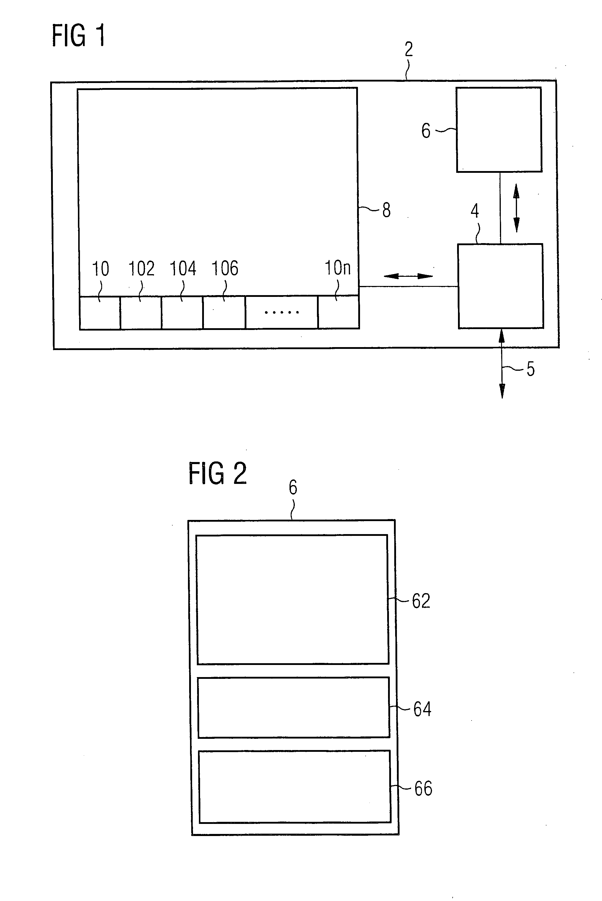
[0032]FIG. 1 shows an embodiment of the present invention. A flash memory device 2 comprises a repository 6 that is associated with a microcontroller 4. The microcontroller 4 has an interface 5 that may connect to an external data or signal source in order to achieve transfer of data to be stored or read out or to communicate with an external test device, etc.
[0033] The microcontroller 4 further operates storage of data in a flash memory array 8, that is based on charge trapping cells and may be of the NAND or NOR-type. The size of the memory 8 may have a wide range adapted to the particular use of the flash device, e.g., 64 Mb with respect to an arbitrary MMC card.
[0034] The repository 6 may be, among other options, of the SRAM type (static RAM), DRAM type (dynamic random access memory) or even the flash type as well. It may have a size of 4 kb with a four times redundancy in order to provide an amount of error tolerance. In other words, each bit of the binary code stored in the ...
PUM
 Abstract
Description
Claims
Application Information


