Method of forming a contact in a flash memory device

a flash memory device and contact technology, applied in the direction of basic electric elements, semiconductor devices, electrical apparatus, etc., can solve the problems of shortening or at least reducing the overlay accuracy budget, and achieve the effect of increasing the yield of flash memory devices, increasing the overlay budget available, and increasing the quality of flash memory devices

Inactive Publication Date: 2008-01-22
POLARIS INNOVATIONS LTD
View PDF15 Cites 2 Cited by
  • Summary
  • Abstract
  • Description
  • Claims
  • Application Information

AI Technical Summary

Benefits of technology

[0015]In one aspect, the present invention increases the quality of flash memory devices. In a further aspect, the present invention increases the yield of flash memory device production. In still a further aspect, the overlay budget available is increased when producing flash memory devices. A still further aspect results in reduced costs and efforts in semiconductor flash memory manufacturing.
[0021]The second dielectric layer is deposited upon the hard mask and also structured in a lithographic step. The corresponding etch mask, e.g., a resist or other hard mask, comprises openings for trenches, which are to form the bitlines. Etching the second dielectric layer down to the hard mask provides the advantage that an automatic etch stop can be achieved, which can be independent of any time control.
[0025]According to a further aspect of the invention a third dielectric layer is deposited upon the planarized surface prior to depositing the first dielectric layer. This further layer may be composed of an oxide, or an oxynitride, if the first dielectric layer is a nitride. This third layer has the advantage to reduce the hard mask thickness and to keep the stack thickness sufficiently large in order to match isolation and capacitance needs.
[0026]Nevertheless, a single layer of only nitride adversely has the advantage of preventing sidewalls of the contact hole from undergoing disadvantageous under-etching.

Problems solved by technology

This misalignment may lead to shorts or at least to a smaller budget of overlay accuracy for the corresponding two lithographic mask processes.

Method used


Image

  • Method of forming a contact in a flash memory device
  • Method of forming a contact in a flash memory device
  • Method of forming a contact in a flash memory device

Examples


Embodiment Construction

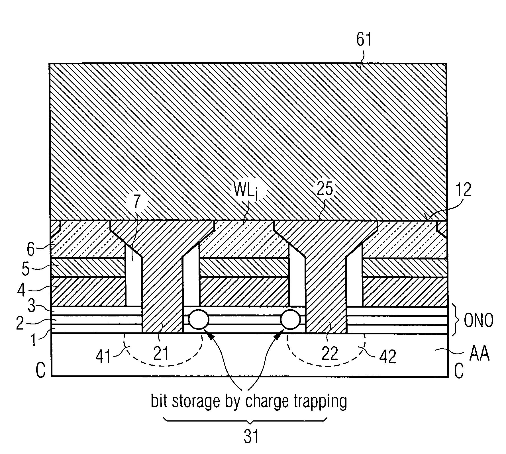
[0070]An embodiment of the method according to the invention is shown with reference to FIGS. 3-9, which display cross sections of the memory array 10 along lines A-A and B-B as indicated in FIG. 1. FIG. 3, which includes FIGS. 3a and 3b, displays an intermediate step of a sequence of steps for manufacturing a memory array according to an embodiment of the invention, the intermediate step serving as a starting point herein in order to explain the details of the invention.

[0071]However, a short overview of the processing steps that lead to the situation shown in FIG. 3 is provided. A series of parallel wordlines WL is formed on the surface of a semiconductor substrate. The wordlines WL may comprise—from bottom to top—a layer sequence of dielectric materials, i.e., an ONO-layer serving as a gate dielectric of the transistor 31 and simultaneously serving as the memory layer 2 being sandwiched by confinement layers 1, 3. A conductive layer of polysilicon 4 forming a gate electrode, a co...


PUM

PropertyMeasurementUnit
thicknessaaaaaaaaaa
thicknessaaaaaaaaaa
thicknessaaaaaaaaaa

Abstract

A method of forming a contact between a bitline and a local interconnect in a flash memory device comprises forming a hard mask layer on a planarized surface that includes an exposed top section of the local interconnects prior to depositing an oxide dielectric layer. The hard mask layer may be composed of a material that has an etch resistance as compared to the interlayer dielectric material, e.g., nitride. Openings in the hard mask define positions for the contacts to the local interconnects exposed in the top section.

Description

TECHNICAL FIELD[0001]The invention relates to a method of forming a contact in a flash memory device. The invention further relates to manufacturing a memory array of a flash memory device. The invention particularly relates to flash memory arrays comprising local interconnects, which provide an electrical connection between source and drain regions of neighboring memory cells.BACKGROUND[0002]Non-volatile memory, or more precisely: flash memory, has become increasingly important for mass storage media, cards and code-products. Memory cells of a flash memory array are based on trapping of charge carriers in a floating gate or in a dielectric memory layer confined by thin confinement layers, e.g., an ONO-layer (Oxide-Nitride-Oxide) sequence. These non-volatile memory cells are electrically programmable and erasable.[0003]Two major flash memory device concepts relate to so-called NOR- or NAND-flash devices. NOR-flash devices are suited for the storage of software and program files due ...

Claims


Application Information

Patent Timeline
Patent Type & Authority Patents(United States)
IPC IPC(8): H01L21/4763
CPCH01L21/76802H01L21/76895H01L27/115H01L27/11568H10B69/00H10B43/30H10B43/10H10B12/00H10B10/00H10B20/00
Inventor NAGEL, NICOLASOLLIGS, DOMINIK
Owner POLARIS INNOVATIONS LTD
Why Eureka
Try Eureka