

LED structure for flip-chip package and method thereof
- Summary
- Abstract
- Description
- Claims
- Application Information
AI Technical Summary
Benefits of technology
Problems solved by technology
Method used
Image

Examples
Embodiment Construction
[0025] Method and structure of LED structure for flip-chip package is described below. In the following description, numerous specific details are set forth in order to provide a thorough understanding of the present invention, and the scope of the present invention is expressly not limited expect as specified in the accompanying claims.
[0026] The components of the different elements are not shown to scale. Some dimensions of the related components are exaggerated and meaningless portions are not drawn to provide clearer description and comprehension of the present invention.
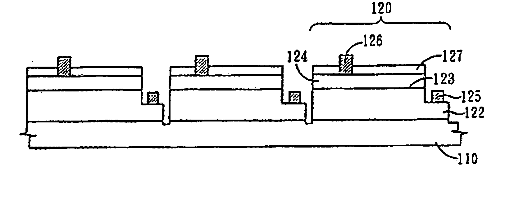
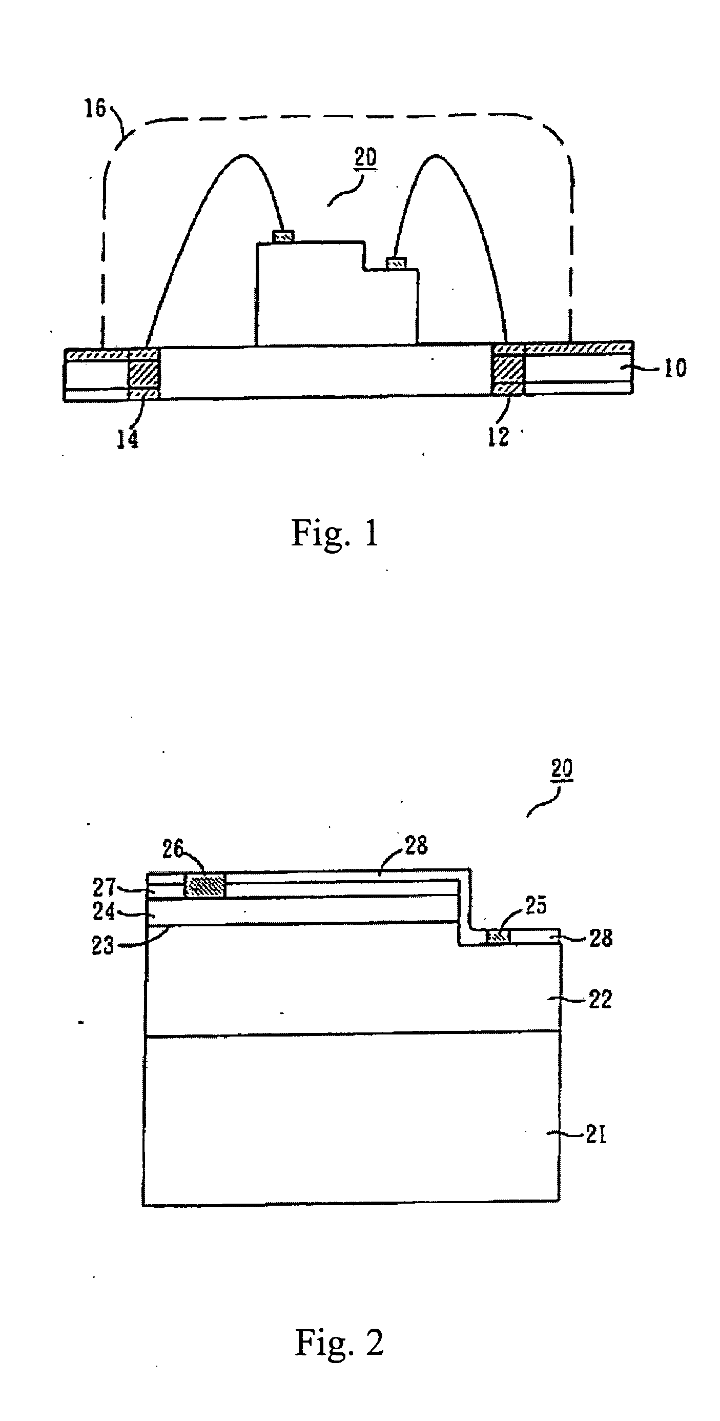
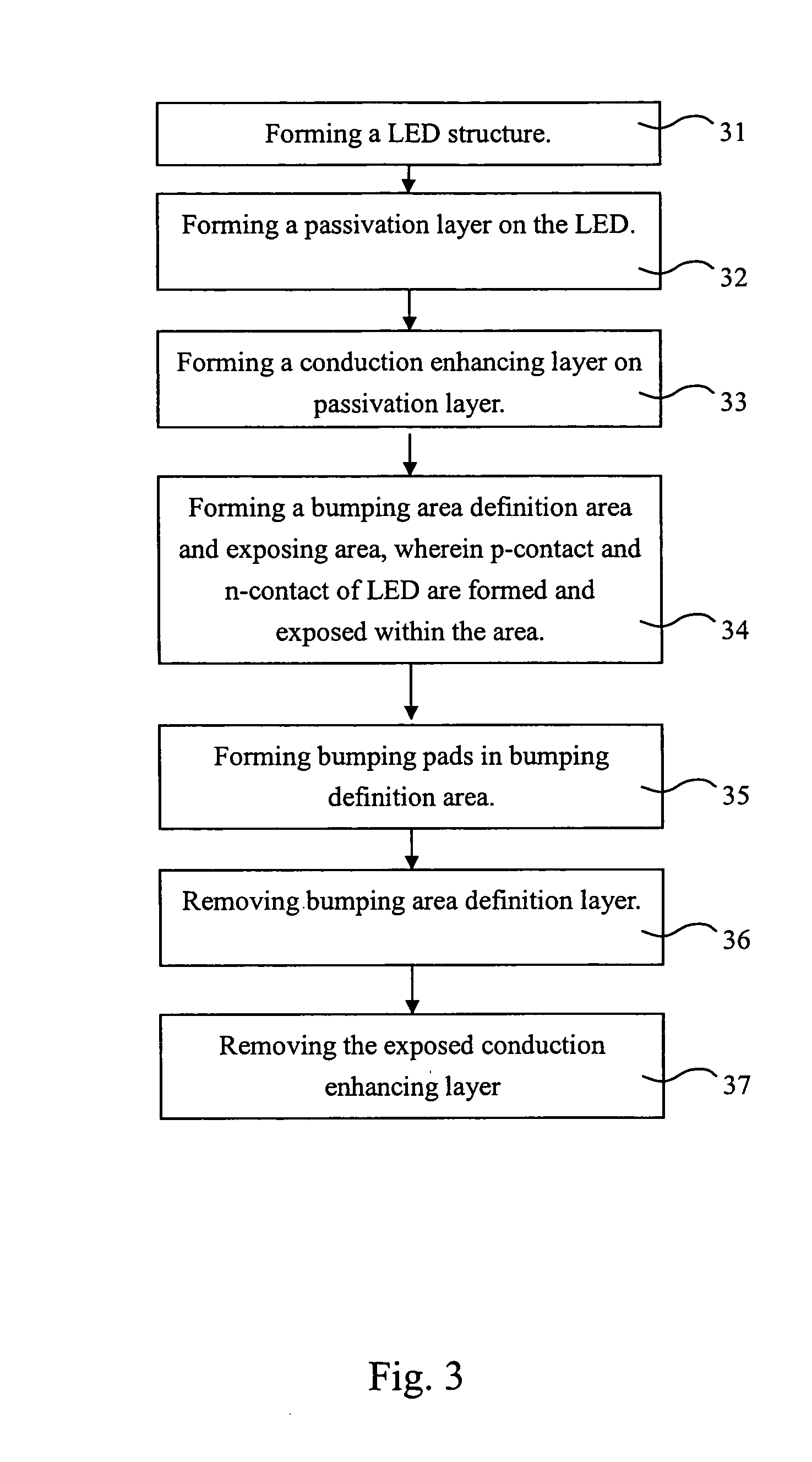
[0027] The present invention is related to a method for making LEDs ready for flip-chip packaging. First, forming a conduction enhancing layer on a LED structure, and connected electrically to p-contact and n-contact of the LED structure. The LED structure is formed on a transparent substrate, and comprises a passivation layer residing on a LED structure. Afterward, forming a bumping area definition layer on a...
PUM
 Abstract
Description
Claims
Application Information