
Optical scanning system with correction

a technology of optical scanning and correction, applied in optics, instruments, electrical equipment, etc., can solve the problems of large power consumption, device limitations, and bulky crts, and is undesirable for portable or head-mounted applications

Inactive Publication Date: 2006-12-21
MICROVISION +1
View PDF69 Cites 86 Cited by
  • Summary
  • Abstract
  • Description
  • Claims
  • Application Information

AI Technical Summary

Benefits of technology

The patent describes a display system that uses a scanning mechanism to produce images in a tile-like manner. The scanning mechanism includes a mirror that sweeps the beams of light horizontally and vertically, creating spatially distinct regions of the image. The number of pixels in each region is determined by the scan angle and the mirror dimensions. The scanning system can be controlled to adjust the drive signals to the optical sources and compensate for variations in output intensity caused by pattern dependent heating. The system also includes a buffer to store data and a control circuit to adjust the resonant frequency of the MEMs scanner. The patent also describes an imager that uses multiple detector / optical source pairs to capture images in different colors and at different wavelengths. The scanning mechanism can be expanded to write more than just two tiles by using multiple input fibers and optical switches.

Problems solved by technology

Such devices suffer from several limitations.
For example, CRTs are bulky and consume substantial amounts of power, making them undesirable for portable or head-mounted applications.
Such screens have limited use in head mounted applications or in applications where the display is intended to occupy only a small portion of a user's field of view.
Such displays have been reduced in size, at the cost of increasingly difficult processing and limited resolution or brightness.
Also, improving resolution of such displays typically requires a significant increase in complexity.
Devices for acquiring images, such as cameras and scanning microscopes may have similar constraints.
In high resolutions systems, the CCD array can be complex.
Full color CCD applications can add further complexity.
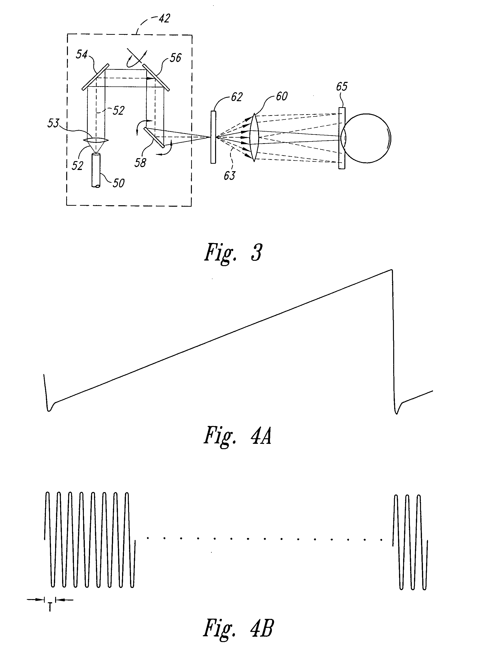
One difficulty that may arise with such displays is raster pinch, as will now be explained with reference to FIGS. 3-5.
Although considerable progress has been made in the fabrication of single refractive microlenses in this regime, the construction of high-power, high-resolution systems of refractive microlenses capable of diffraction limited imagery over a large field of view remains a considerable technological challenge.
This can add considerable complexity for the micro-optical instrument, and in many cases a practical design may not be realized.
This uneven spacing can cause the pixels to overlap or can leave a gap between adjacent rows of pixels.
Moreover, because the image information is typically provided as an array of data, where each location in the array corresponds to a respective position in the ideal raster pattern 69, the displaced pixel locations can cause image distortion.
Further optical aberrations in the optical train may produce pixel non-uniformities, distortion, or other artifacts that may reduce the appearance or degrade the performance of a scanned display or image capture device.

Method used


Image

  • Optical scanning system with correction
  • Optical scanning system with correction
  • Optical scanning system with correction

Examples


Embodiment Construction

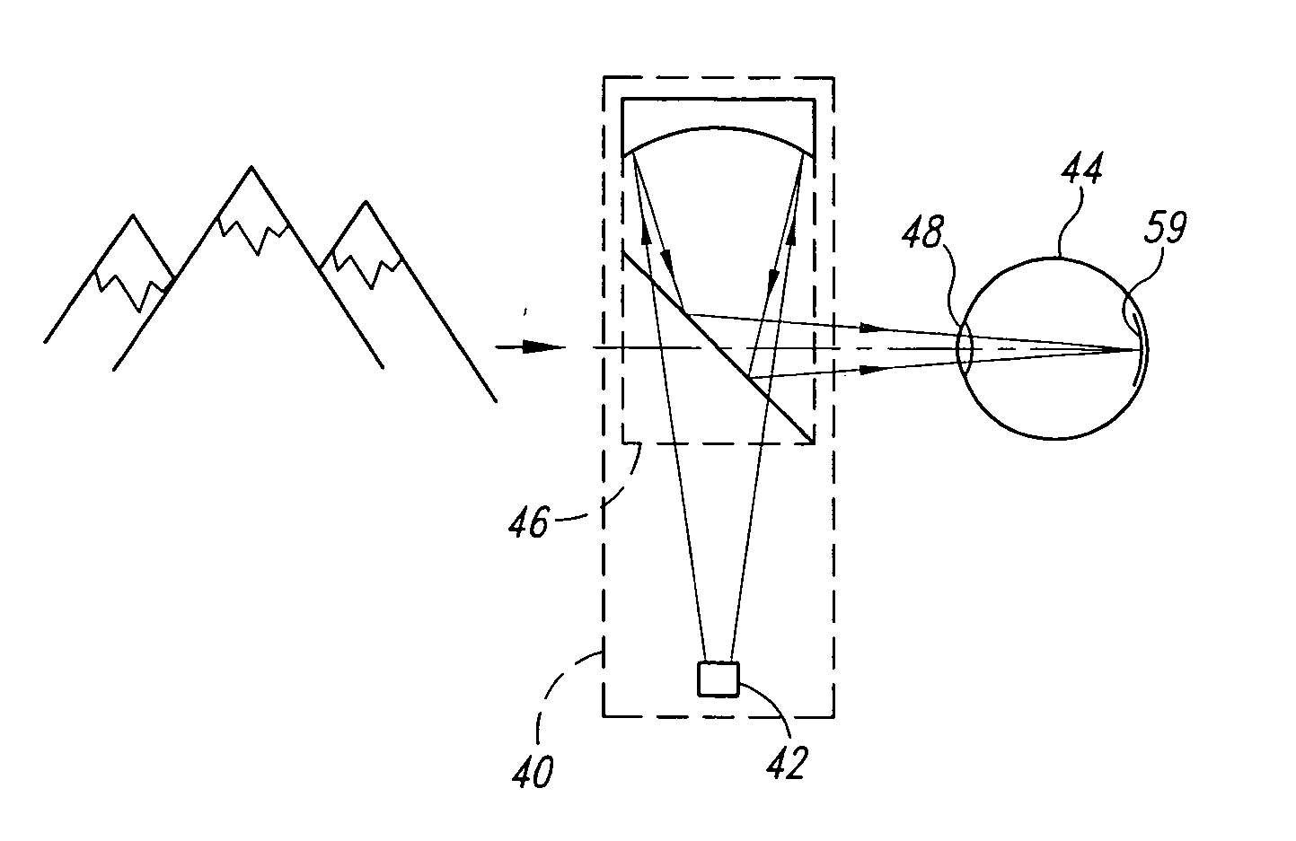
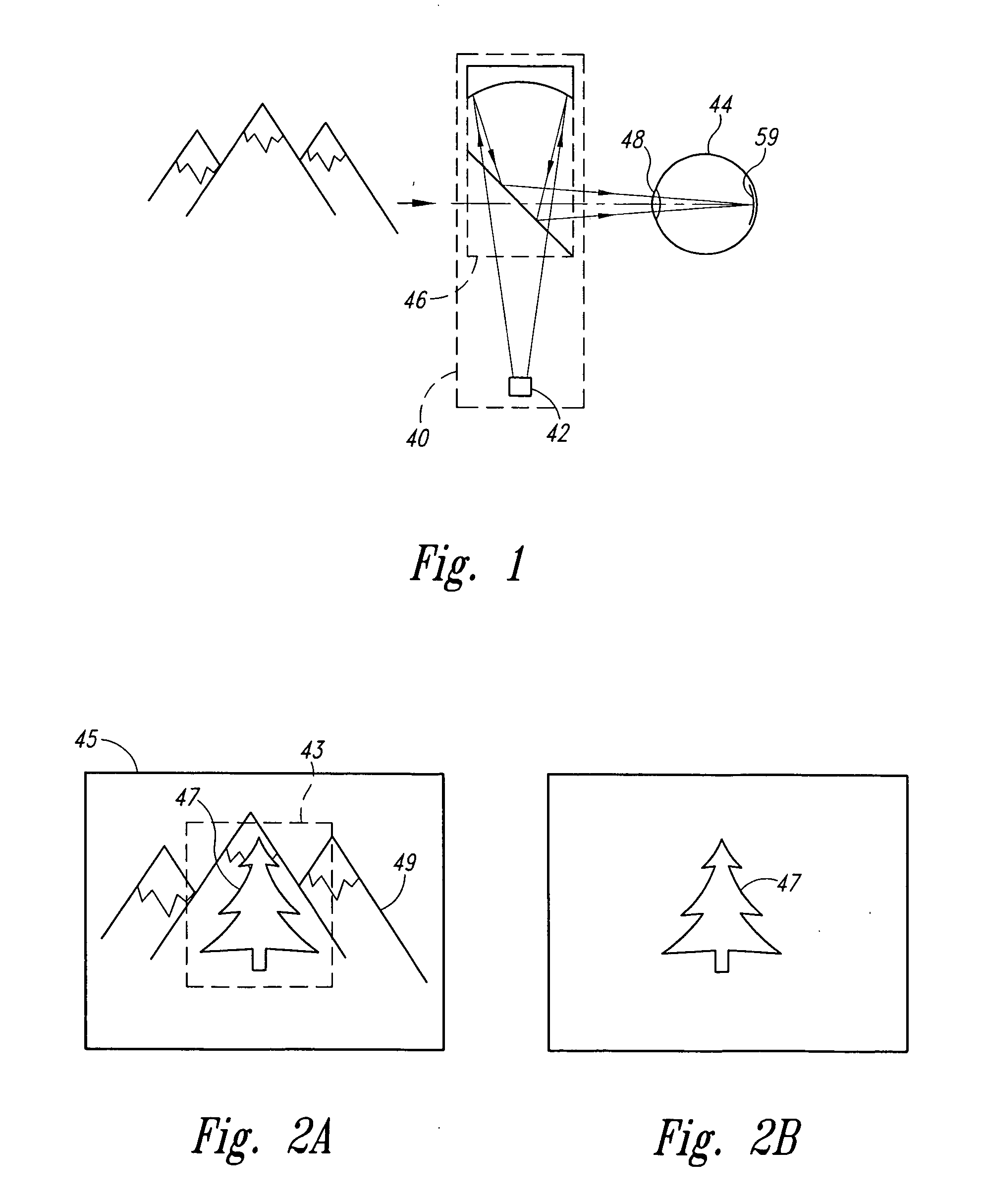
[0088] As shown in FIG. 6, a scanned beam display 70 according to one embodiment of the invention is positioned for viewing by a viewer's eye 72. While the display 70 is presented herein is scanning light into the eye 72, the structures and concepts described herein can also be applied to other types of displays, such as projection displays that include viewing screens. Moreover, the invention is not limited to scanned beam displays. For example, as will be described below, image capture devices or optical switches may also be within the scope of the invention.

[0089] The display 70 includes four principal portions, each of which will be described in greater detail below. First, control electronics 74 provide electrical signals that control operation of the display 70 in response to an image signal VIM from an image source 76, such as a computer, television receiver, videocassette player, DVD player, remote sensor, or similar device.

[0090] The second portion of the display 70 is a ...


PUM


Abstract

A scanning system device has a predetermined aberration as it scans or switches light along selected optical paths. A deformable membrane receives the light and introduces an inverse “aberration” that offsets that of the scanning system. In one embodiment the scanning system includes a torsion arm that supports an oscillatory body. The torsion arm and / or body can be machined from metal, micromachined in silicon or formed in a variety of other ways. Alternatively, the scanning system may include a rotating polygonal scanner or other type of optical scanner. In another approach, an optical switch replaces the scanner.

Description

RELATED APPLICATIONS [0001] This application is a continuation-in-part of U.S. patent application Ser. No. 09 / 129,252, filed Aug. 5, 1998.TECHNICAL FIELD [0002] The present invention relates to scanned light devices and, more particularly, to scanned light beam displays and imaging devices for viewing or collecting images. BACKGROUND OF THE INVENTION [0003] A variety of techniques are available for providing visual displays of graphical or video images and for acquiring images. In many display applications, cathode ray tube type displays (CRTs), such as televisions and computer monitors produce images for viewing. Such devices suffer from several limitations. For example, CRTs are bulky and consume substantial amounts of power, making them undesirable for portable or head-mounted applications. [0004] Matrix addressable displays, such as liquid crystal displays and field emission displays, may be less bulky and consume less power. However, typical matrix addressable displays utilize ...

Claims


Application Information

Patent Timeline
Patent Type & Authority Applications(United States)
IPC IPC(8): G09G5/00
CPCG02B26/10G02B26/101G02B27/0031G02B27/01G02B27/0101H04N2201/0476G02B2027/014G09G3/02H04N1/047H04N2201/0471H04N2201/04744G02B2027/011
Inventor TEGREENE, CLARENCE T.DICKENSHEETS, DAVID L.
Owner MICROVISION
Learn More