Display panel, display device equipped with the same, and display device manufacturing method

a technology for display devices and display panels, applied in non-linear optics, instruments, optics, etc., can solve problems such as insufficient removal of shorting interconnections, line defects, and shorting, and achieve the effect of increasing manufacturing costs, easy and precisely measuring the amount of beveling

Inactive Publication Date: 2006-12-21
MITSUBISHI ELECTRIC CORP
View PDF10 Cites 7 Cited by
  • Summary
  • Abstract
  • Description
  • Claims
  • Application Information

AI Technical Summary

Benefits of technology

[0013] In the manufacture of a display device, an object of the invention is to make it possible to easily and pr

Problems solved by technology

This process causes so large amounts of static electricity that overvoltage may be applied to the scanning interconnections and signal interconnections, which may lead to breakage of switching elements and hence occurrence of line defects.
However, in the beveling process, the shorting interconnection may be insufficiently removed because of variations of the amount of beveling.
Then, fragments of the shorting interconnection remaining unremoved will cause short-circuits between adjacent interconnections, leading to display defects like line d

Method used


Image

  • Display panel, display device equipped with the same, and display device manufacturing method
  • Display panel, display device equipped with the same, and display device manufacturing method
  • Display panel, display device equipped with the same, and display device manufacturing method

Examples


first preferred embodiment

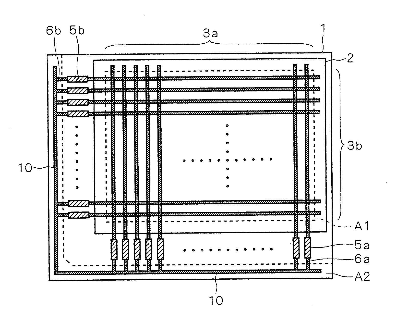
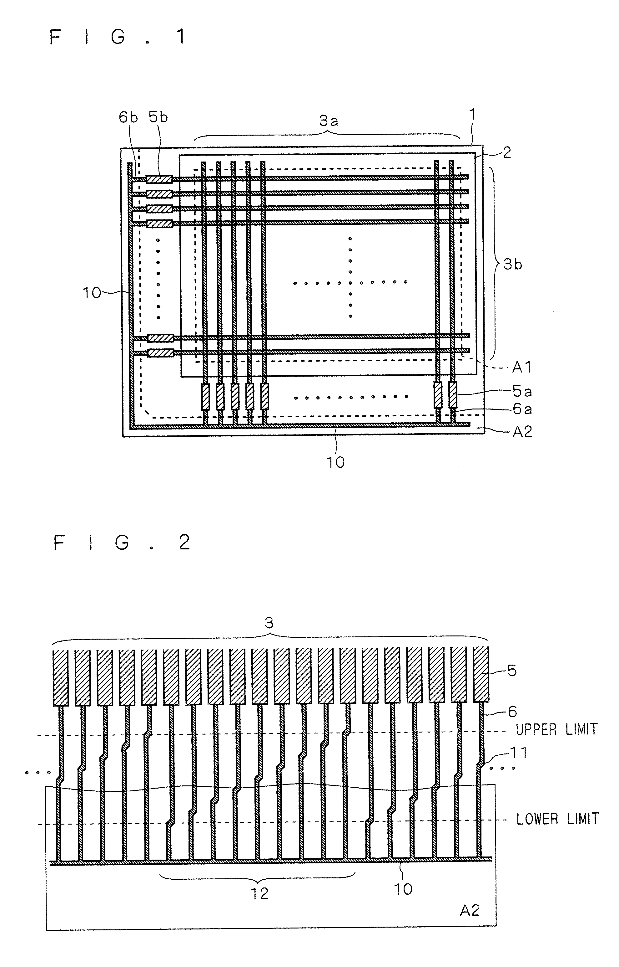
[0023] The structure of a display device according to a preferred embodiment will now be described. The description herein shows a TFT liquid-crystal display device as a display device to which the present invention is applied. FIG. 1 is a plan view of a display panel (liquid-crystal panel) of the display device of the invention. FIG. 1 shows the display panel from which a shorting interconnection has not yet been removed. The beveled area A2 including the shorting interconnection 10 shown in FIG. 1 is removed by beveling when the display panel is attached to the display device (for example, before an image inspection process).

[0024] This display panel includes a first substrate 1 and a second substrate 2 sandwiching liquid crystal as display material. On the first substrate 1, a plurality of parallel signal interconnections 3a and a plurality of parallel scanning interconnections 3b are formed. The signal interconnections 3a and the scanning interconnections 3b are arranged so tha...

second preferred embodiment

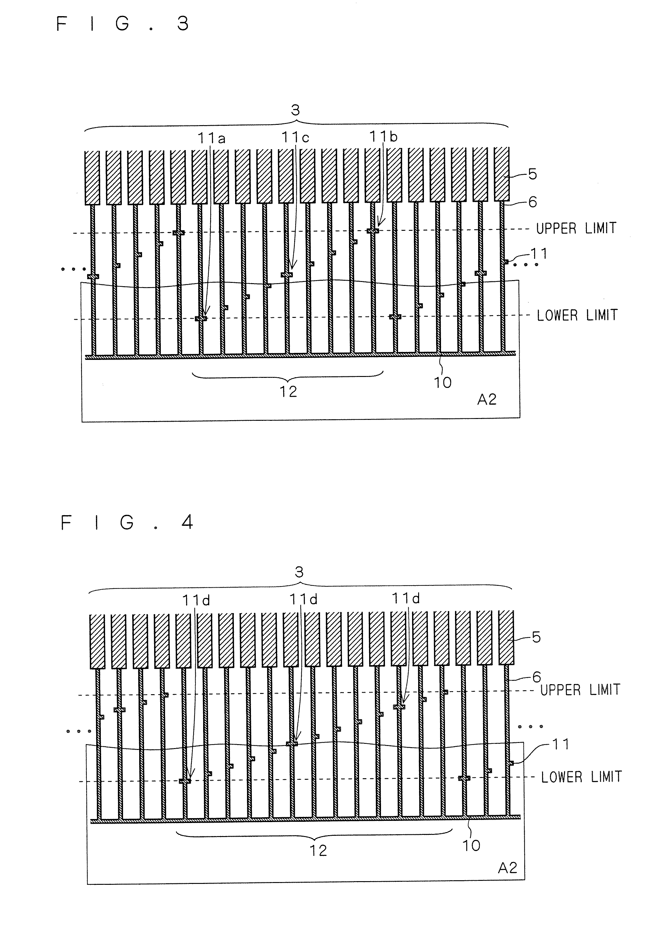
[0042]FIG. 3 is a diagram used to describe the structure of a display device according to a second preferred embodiment of the present invention. FIG. 3 is an enlarged view showing a beveled area A2 and its vicinity along an edge of the display panel. In FIG. 3, the elements having the same functions as those of FIGS. 1 and 2 are shown at the same reference characters. As shown in FIG. 3, the structure of the display device of this preferred embodiment differs from that of the first preferred embodiment (FIG. 2) in the shape of the marks 11. The structures are the same in other respects.

[0043] As shown in FIG. 3, the marks 11 are provided only in the region between the upper limit and lower limit positions of beveling (within a specified range). That is, among the marks 11, the one located in the outermost position on the first substrate 1 (the mark 11a) corresponds to the lower limit position and the innermost one (the mark 11b) corresponds to the upper limit position. In this pre...

third preferred embodiment

[0047]FIG. 4 is a diagram used to describe the structure of a display device according to a third preferred embodiment of the present invention. FIG. 4 is an enlarged view showing a beveled area A2 and its vicinity along an edge of the display panel. In FIG. 4, too, the elements having the same functions as those of FIGS. 1 and 2 are shown at the same reference characters. As shown in FIG. 4, the structure of the display device of this preferred embodiment differs from that of the first preferred embodiment (FIG. 2) in the shape of the marks 11. For convenience of description, the unit cycle pattern 12 of FIG. 4 includes an increased number of, 13, interconnections 3.

[0048] As shown in FIG. 4, the marks 11 are provided only in the region between the upper limit and lower limit positions of beveling (within a specified range). In this preferred embodiment, in the unit cycle pattern 12, marks 11 (marks 11d) of particular interconnections 3 separated by a given number of interconnecti...


PUM


Abstract

In the manufacture of a display device, an object of the invention is to make it possible to easily and precisely measure the amount of beveling of the display panel without an increase in manufacturing costs. In the process of manufacturing a display device, a shorting interconnection (10) is provided near edges of the display panel in order to short-circuit signal interconnections and scanning interconnections (interconnections 3). In a final stage, the shorting interconnection (10) is removed together with a beveled area (A2) by the beveling of the edges of the display panel. The interconnections (3) have marks (11) that are formed near the edges of the substrate and used as reference for the amount of beveling. Each mark (11) is located in a position shifted from the mark (11) of an adjacent interconnection (3) along the length of the interconnections (3).

Description

BACKGROUND OF THE INVENTION [0001] 1. Field of the Invention [0002] The present invention relates to a display device having a display panel formed of a pair of substrates and a display material, such as liquid crystal, sandwiched therebetween. [0003] 2. Description of the Background Art [0004] In a display panel (liquid-crystal panel) of a liquid-crystal display device, a liquid-crystal material is sandwiched between a pair of substrates, and a plurality of signal interconnections and scanning interconnections, perpendicular to each other, are provided on the panel. In the display panel, pixels are formed at the intersections of the signal interconnections and the scanning interconnections. [0005] For example, in an active-matrix display panel in which each pixel has a switching element (also called “an active component”) such as a thin film transistor (TFT), the signal interconnections, scanning interconnections, and switching elements are formed on one of the two substrates. Pixe...

Claims


Application Information

Patent Timeline
IPC IPC(8): G02F1/1345
CPCG02F1/136204G02F1/1345
Inventor TERAMOTO, KENJI
Owner MITSUBISHI ELECTRIC CORP
Why Eureka
Try Eureka