Liquid crystal display device and manufacturing method thereof

a technology of liquid crystal display and manufacturing method, which is applied in non-linear optics, instruments, optics, etc., can solve the problems of inability to increase the arrangement density of columnar spacers so high, and the columnar spacers cannot follow deformation, etc., and achieves high quality

Active Publication Date: 2006-12-21
SHARP KK
View PDF14 Cites 31 Cited by
  • Summary
  • Abstract
  • Description
  • Claims
  • Application Information

AI Technical Summary

Benefits of technology

[0031] The invention can realize a high quality liquid cry

Problems solved by technology

However, when the density of the columnar spacers is made too high, when a volume of the liquid crystal decreases under low temperatures, the columnar spacers cannot follow to deform.
Accordingly, there is a problem in that, inside of the liquid crystal display panel, a vacuum area is generated and therein an air bubble is generated.
As a result, the arrangement density of the columnar spacers cannot be increased so high, that is, t

Method used


Image

  • Liquid crystal display device and manufacturing method thereof
  • Liquid crystal display device and manufacturing method thereof
  • Liquid crystal display device and manufacturing method thereof

Examples


first embodiment

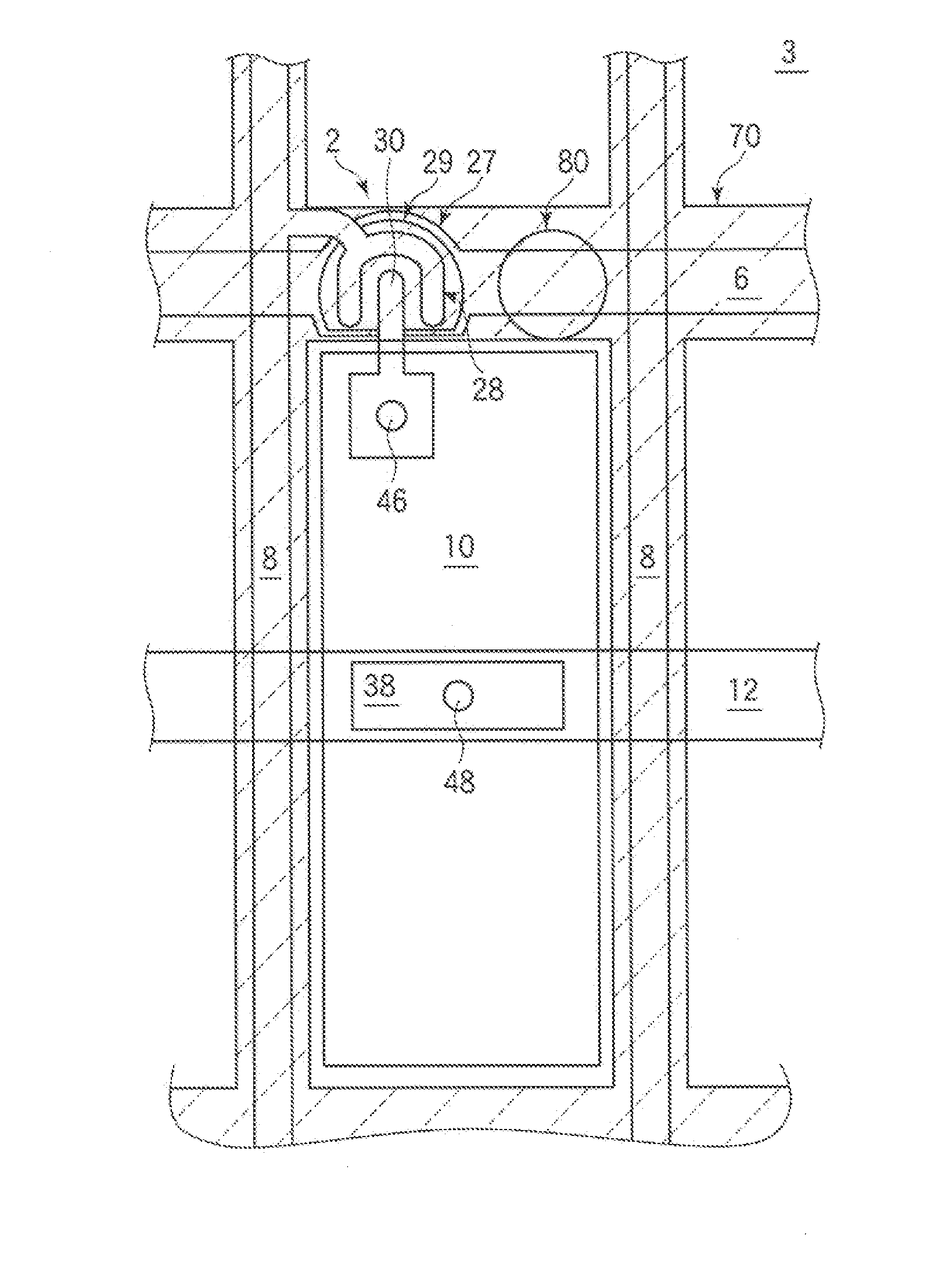
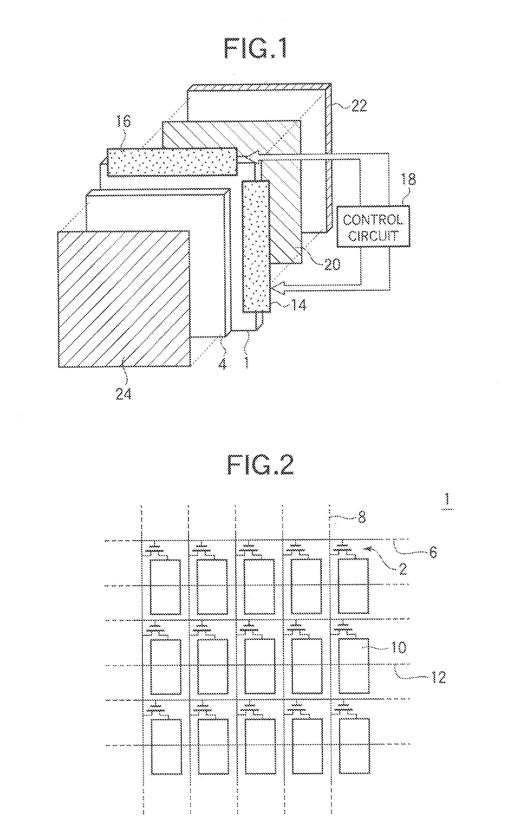
[0053] A liquid crystal display device according to a first embodiment of the invention and a manufacturing method thereof will be described with reference to FIGS. 1 through 6. In the beginning, a schematic configuration of the liquid crystal display device according to the embodiment will be described with reference to FIGS. 1 through 3. FIG. 1 shows a schematic configuration of the liquid crystal display device according to the embodiment. FIG. 2 shows an equivalent circuit of elements formed on a thin film transistor (TFT) substrate 1. As shown in FIGS. 1 and 2, a liquid crystal display device has a structure where a TFT substrate (array substrate) 1 on which TFTs 2 are formed and an opposite substrate 4 on which a common electrode is formed are faced and adhered and liquid crystal is sealed therebetween.

[0054] As shown in FIG. 2, on the TFT substrate 1, a plurality of gate bus lines 6 extending in a horizontal direction in the drawing is formed in parallel with each other and ...

second embodiment

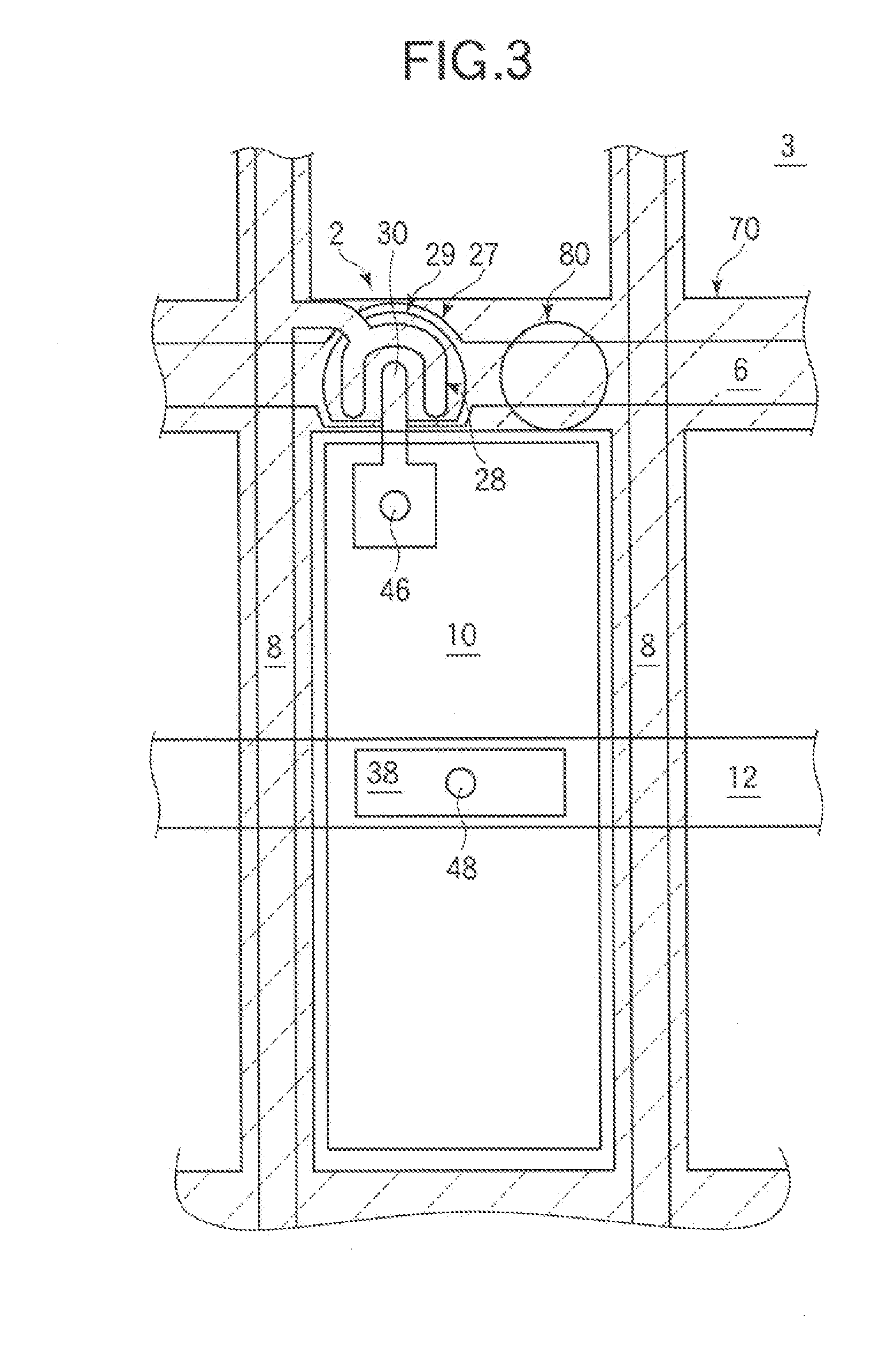
[0069] A liquid crystal display device according to a second embodiment of the invention and a manufacturing method thereof will be described with reference to FIGS. 7 through 9. A schematic configuration of a liquid crystal display device according to the embodiment is similar to that of the liquid crystal display device according to the first embodiment; accordingly, a description thereof will be omitted. FIG. 7 shows a plan layout of one pixel of a TFT substrate (second substrate) 1, which is seen through an opposite substrate (first substrate) 4 of the liquid crystal display device of the embodiment. FIG. 8 shows a section cut along a virtual line A-A′ shown in FIG. 7. FIG. 9 shows a section cut along a virtual line B-B′ shown in FIG. 7.

[0070] As shown in FIGS. 7 through 9, on a glass substrate 3 as a transparent insulating substrate, directly or as needs arise after a protective film such as SiOx is formed, for instance, Al (aluminum) or an Al alloy (not shown in the drawing) ...

third embodiment

[0081] A liquid crystal display device according to a third embodiment of the invention and a manufacturing method thereof will be described with reference to FIGS. 10 through 12. A schematic configuration of a liquid crystal display device according to the embodiment is similar to that of the liquid crystal display device according to the first embodiment; accordingly, a description thereof will be omitted. FIG. 10 shows a plan layout of one pixel of a TFT substrate (second substrate) 1, which is seen through an opposite substrate (first substrate) 4 of the liquid crystal display device of the embodiment. FIG. 11 shows a section cut along a virtual line A-A′ shown in FIG. 10. FIG. 12 shows a section cut along a virtual line B-B′ shown in FIG. 10.

[0082] As shown in FIGS. 10 through 12, on a glass substrate 3 as a transparent insulating substrate, directly or as needs arise after a protective film such as SiOx is formed, for instance, Al or an Al alloy (not shown in the drawing) wit...


PUM


Abstract

The invention relates to a liquid crystal display device that is used in display portions of electronics devices and a manufacturing method thereof, and an object is to provide a high quality liquid crystal display device where light is inhibited from leaking and a manufacturing method thereof. The projected structure formed of the first through the fourth columnar spacer receiving patterns, the insulating film and the final protective film is formed on the TFT substrate. The projected structure is buried in the columnar spacer disposed on the opposite substrate. Thereby, even when the liquid crystal display panel is surface pressed, both substrates are hardly displaced.

Description

BACKGROUND OF THE INVENTION [0001] 1. Field of the Invention [0002] The invention relates to a liquid crystal display device that is used in display portions of electronics devices and a manufacturing method thereof. [0003] 2. Description of the Related Art [0004] A liquid crystal display device is advantageous in comparison with a CRT (Cathode Ray Tube) in that it is thin, light, capable of driving at lower voltages and low in the power consumption. Accordingly, the liquid crystal display device is used in display portions of various kinds of electronics devices such as TV receivers, note-type PCs (personal computers), desktop computers, PDAs (portable terminal assistants) and portable telephones. In particular, an active matrix liquid crystal display device where a TFT (Thin Film Transistor) is disposed as a switching element to each of pixels (sub-pixels) shows excellent display characteristics comparative to the CRT owing to high drivability and has become being widely used in f...

Claims


Application Information

Patent Timeline
IPC IPC(8): G02F1/1339G02F1/136
CPCG02F1/13394
Inventor MISAKI, KATSUNORISAWASAKI, MANABUKUROSAWA, YOSHIO
Owner SHARP KK
Why Eureka
Try Eureka