Stacked microelectronic assemblies having basal compliant layers

Inactive Publication Date: 2006-12-21
TESSERA INC
View PDF13 Cites 21 Cited by
  • Summary
  • Abstract
  • Description
  • Claims
  • Application Information

AI Technical Summary

Benefits of technology

[0022] Although the present invention is not limited by any particular theory of operation, it is believed that providing a compliant layer for the bottom-most chip of a stacked assembly, while not providing a compliant layer f

Problems solved by technology

When chips are stacked one atop the other, it is difficult to dissipate the heat generated by the chips in the middle of the stack.
Consequently, the chips in such a stack may undergo substantial

Method used


Image

  • Stacked microelectronic assemblies having basal compliant layers
  • Stacked microelectronic assemblies having basal compliant layers
  • Stacked microelectronic assemblies having basal compliant layers

Examples


Example

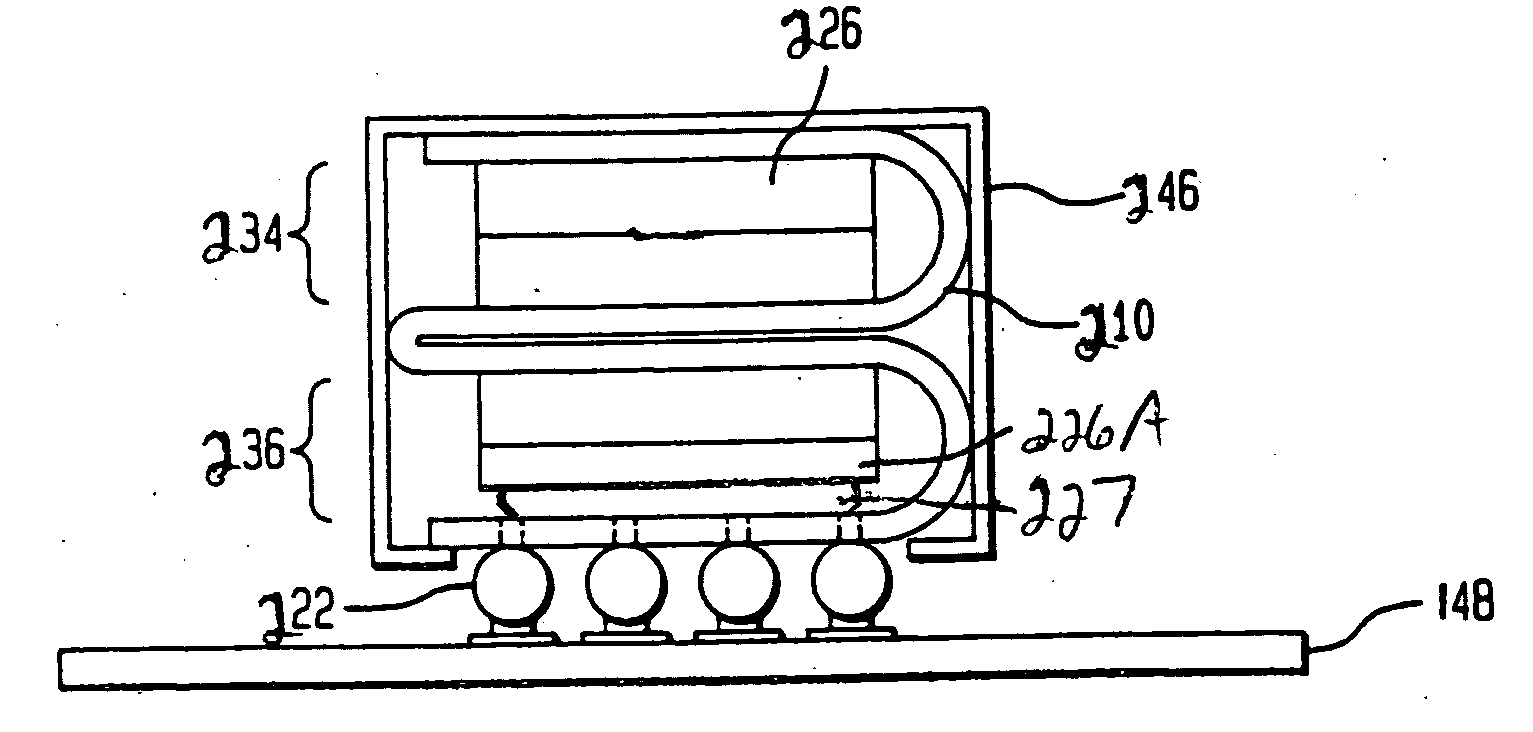
[0040] As noted above, the present invention is related to providing a basal compliant layer for a stacked microelectronic assembly. In certain preferred embodiments, only the bottom microelectronic element in a stack has a compliant layer for enabling movement during thermal cycling, while the microelectronic elements above the bottom microelectronic element do not have a compliant layer. This design reduces the overall height of the stacked package, while allowing movement between the bottom-most microelectronic element and the conductive terminals of the assembly.

[0041] Referring to FIGS. 6 and 7, in certain preferred embodiments of the present invention, a stacked assembly includes a plurality of chips 126 mounted to a flexible substrate 100. The substrate 100 is folded to align the chips 126 in a generally vertical configuration. An adhesive 144, such as a thermally conductive adhesive, is provided between juxtaposed back surfaces 132 of semiconductor chips 126. The adhesive 1...


PUM


Abstract

A method of making a stacked microelectronic assembly includes providing a flexible substrate having first and second ends, the flexible substrate having a plurality of attachment sites located between the first and second ends thereof including a first one of the attachment sites located adjacent the first end of the flexible substrate, the flexible substrate including conductive terminals accessible at a surface of the flexible substrate and wiring connected to the terminals, providing a compliant layer over the first attachment site, assembling a plurality of microelectronic elements over the attachment sites, wherein a first one of the microelectronic elements engages the compliant layer and is movable relative to the flexible substrate, electrically interconnecting the microelectronic elements and the wiring, folding the flexible substrate and stacking at least some of the microelectronic elements in generally vertical alignment with one another so that the first one of the microelectronic elements engaging the compliant layer is disposed at a bottom of the stacked assembly, and maintaining the stacked microelectronic elements in the substantially vertical alignment, wherein the conductive terminals are exposed at the bottom end of the stacked assembly.

Description

FIELD OF THE INVENTION [0001] The present invention relates to microelectronic assemblies and more particularly relates to stacked microelectronic assemblies having compliant layers. BACKGROUND OF THE INVENTION [0002] Semiconductor chips are commonly provided as individual, prepackaged units. A standard chip has a flat, rectangular body with a large front face having contacts for connection to the internal circuitry of the chip. Each individual chip is typically mounted to a substrate or chip carrier, which in turn is mounted on a circuit panel such as a printed circuit board. Considerable effort has been devoted towards development of so-called “multichip packages” in which several chips having related functions are attached to a common circuit panel and protected by a common package. This approach conserves some of the space which is ordinarily wasted by individual chip packages. However, most multichip packages utilize a single layer of chips positioned side-by-side on a surface ...

Claims


Application Information

Patent Timeline
IPC IPC(8): H01L21/00
CPCH01L23/5387H01L25/0657H01L2225/107H01L2224/16225H01L2225/06513H01L25/105
Inventor SOLBERG, VERNONBELLAAR, PIETER H.KIM, YOUNG-GONHABA, BELGACEM
Owner TESSERA INC
Why Eureka
Try Eureka